
Circuit Diagram
Index 1923
TMP87C054-7222 monolithic microcomputer integrated circuit diagram
Published:2011/5/9 1:25:00 Author:Ecco | Keyword: monolithic, microcomputer , integrated circuit


TMP87C054-7222 is the single-chip microcomputer IC produced by Toshiba in Japan, it is widely used in Haier, Toshiba, and other series of both large-screen color TV. TMP87C054-7222 integrated circuit uses the package with 54 feet in double rows, the pin-letter codes and data are listed in Table 1, the internal block diagram and pin functions and signal flowing are shown in Figure 1.
(View)
View full Circuit Diagram | Comments | Reading(602)
Typical applied Circuit Diagram of M54123 Intergrated Circuit
Published:2011/5/9 19:29:00 Author: | Keyword: Intergrated Circuit

Typical Applied Circuit Diagram
Typical applied circuit diagram of leakage protecter composed of M54123 IC is demonstrated as the abboved picture.
Picture:The typical applied circuit diagram of M54123 IC
Note:China's homegrown part number of M54123 IC is SF4123 and they can be used interchangeably directly. (View)
View full Circuit Diagram | Comments | Reading(2679)
TMS73C167 monolithic microcomputer integrated circuit diagram
Published:2011/5/9 1:15:00 Author:Ecco | Keyword: monolithic , microcomputer , integrated circuit


TMS73C167 is the single-chip microcomputer integrated circuit produced by Toshiba, it is widely used in Toshiba, Konka series. 1. Features of functionsTMS73C167 integrated circuits is mainly composed of the central processing unit (CPU), clock oscillator circuit, the reset control circuit, the key bit instruction decoding circuit, I2C bus control circuit, remote control command signal processing circuit, standby-on control circuit, squelch control circuit, the display character generator and handling circuit, and other auxiliary functions circuit.2. Pin functions and data TMS73C167 integrated circuit uses the package with 54 feet in double rows, the pin functions and signal flowing are shown in Figure 1, the pin letter code and data are listed in Table 1.
(View)
View full Circuit Diagram | Comments | Reading(812)
Constant current battery charger circuit
Published:2011/5/7 12:05:00 Author:John | Keyword: Constant current, battery charger

A three-terminal adjustable output voltage regulator can compose a variety of integrated battery chargers. Figure 1 is a constant current battery charger. The circuit is identical with the constant current source. As resistance for resistor R is 24Ω, the output current Io = 1.25/24 = 52mA. It means that 52mA constant current is used to charge the battery. Changes for resistance value of R can result in different charging current. (View)
View full Circuit Diagram | Comments | Reading(1070)
12V constant voltage battery charger circuit
Published:2011/5/7 12:12:00 Author:John | Keyword: constant voltage, battery charger

Figure 1 is a 12V constant voltage charger circuit. The circuit is the basically same with a constant power supply. Resistor R1 is 0.2Ω. R1 is used for limiting. It is equivalent to increase the internal resistance of the charger. The charging rate of the initial phase can be reduced. And integrated overcurrent protection on the regulator can be achieved. (View)
View full Circuit Diagram | Comments | Reading(1054)
TMP47C1638AU353 monolithic microcomputer integrated circuit diagram
Published:2011/5/9 1:20:00 Author:Ecco | Keyword: monolithic , microcomputer , integrated circuit


TMP47C1638AU353 is the single-chip microcomputer integrated circuit produced by Toshiba, it is widely used as the system controlling in Changhong NC-3 large screen color TV movement . 1. Features of functionsTMP47C1638AU353 IC is the core of the system control circuit, which includes the data bus (I2C) way, on-line scanning and field scanning circuit, decoder circuit, the main screen AV switch circuit, the audio signal processing circuit, PIP AV switch circuit, high frequency tuner and other circuits to control. The IC's internal circuit block diagram is shown in Figure 1.
2. Pin functions and data TMP47C1638AU353 integrated circuit uses the package with 54 feet, the pin functions and signal flowing are shown in Figure 1, the pin letter code and data are listed in Table 1.
(View)
View full Circuit Diagram | Comments | Reading(658)
current limiting battery charger circuit
Published:2011/5/7 12:28:00 Author:John | Keyword: battery charger, current limited protection

Figure 1 is a current limiting battery charger. VT transistor and resistor R3 form the limiting network. According to the figure, resistor R3 is a base-emitter power resistor of the transistor VT. It is connected in series with rechargeable batteries. Charging current flows through resistor R3. When the charge current is too large, the voltage drop on R3 exceeds 0.6V, the transistor VT can be conducted. As resistor R2 is in parallel with VT, the conduction of VT leads to the reduction of the equivalent parallel resistance. The output voltage Uo reduces and the output current decreases. So the purpose of limiting charging current is achieved. When taking R3 = lΩ), the maximum charge current is Iom = 0.6 / 1 = 0.6A. Select the R3 of a smaller resitance, so charging current can be larger. But the charging current can not exceed the maximum output current value of the integrated voltage regulator. (View)
View full Circuit Diagram | Comments | Reading(1180)
Signal Circuit of Duty Ratio Ajustable Clock Consisting of 4 NAND gates
Published:2011/5/7 7:30:00 Author:Joyce | Keyword: Signal, Duty Ratio Ajustable, Clock , Consisting of 4 NAND gates
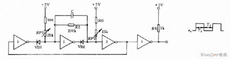
As shown in graph, the circuit is composedof four NAND gates. Oscillation signal frequency is decided by C and the value of potentiometer RP1. RP2 . Changing the resistance of potentiometer can change the frequency whose adjustment range can be 20:1.The resistance of potentiometer RP2 sets the width of output waveform T1 ,and the resistance of potentiometer RP2 sets the width of the output waveform T2.
(View)
View full Circuit Diagram | Comments | Reading(539)
High precision remote temperature measurement circuit
Published:2011/5/7 13:07:00 Author:John | Keyword: reemote temperature measurement circuit

Precision temperature measurement circuit composed of ISO120 and XTR101 is mainly used in remote temperature measurement with a high temperature measurement accuracy. It can also be used for situations with strong noise. ISO120 is a new isolation amplifier, which is designed through the duty factor modulation / demodulation technology. Isolation layer is a two-matched lpF differential capacitor. Digital signals are transmitted. Transmittion of digital signal will not affect the integrity of signals caused by the isolated components. It also has a rather good high-frequency transient performance. Figure shows precision temperature measurement circuit constituted by ISO120 and XTR101. Low temperature drift XTR101 is a 4 ~ 20mA transmitter, and RTD is a thermal resistance. Circuit parameters can guarantee the output current at 4mA in the low temperature end and at 20mA in the high temperature end. Twisted pair will transforme the current to INA105. The current will be converted into electrical signals, then be output through ISO120. (View)
View full Circuit Diagram | Comments | Reading(1117)
Temperature measuring circuit diagram composed of AD7714 and thermocouple
Published:2011/5/6 4:15:00 Author:Ecco | Keyword: Temperature measurement circuit , thermocouple

Temperature measuring circuit diagram composed of AD7714 5-channel low-power programmable sensor signal processor and thermocouple
Temperature measuring circuit diagram composed of AD7714 and thermocouple is shown as the chart. In this application, AD7714 operates in buffered mode, which allows the former termination connecting decoupling capacitors to filter out the noise on the thermocouple leads. In buffered mode, AD7714 common-mode is narrow, the differential thermocouple voltage is in the appropriate range of the common-mode voltage, AD7714's AIN2 input should be biased to +2.5 V reference voltage. (View)
View full Circuit Diagram | Comments | Reading(913)
Spread Spectrum Rolling code Wireless Tracking Alarm Components KB318/KB318R
Published:2011/5/9 10:22:00 Author:TaoXi | Keyword: Spread Spectrum, Rolling code, Wireless Tracking, Alarm Components
The spread spectrum rolling code wireless tracking alarm component can be used in the situations that need the long distance wireless BP machine type feedback alarm such as the cars, motorcycles and other, it uses the advanced technology and devices, so it has the perfect functions and is better than other similar products. The spread spectrum rolling code wireless tracking alarm component is composed of a wireless transmitter KB318T (or KB923T), and a key buckle type micro receiving alarm KB318R (or KB923R). The remote control transmitter principle figure is as shown: (View)
View full Circuit Diagram | Comments | Reading(428)
Pressure measuring system circuit diagram composed of AD7714
Published:2011/5/6 4:10:00 Author:Ecco | Keyword: Pressure measuring system
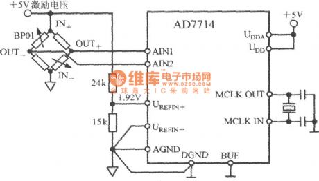
Pressure measuring system circuit diagram composed of AD7714 5-channel low-power programmable sensor signal processor
Pressure measuring system circuit diagram composed of AD7714 is shown as the chart. BP01 is pressure sensor produced by Sensym. The BP01 is connected into a bridge circuit, the OUT +, OUT- ends output differential voltage. When pressure sensor is set the full scale rated pressure (in this case it is 40kPa), its differential output voltage sensitivity is 3mV / V. If it uses +5 V excitation voltage, the sensor full-scale output range is ± 15mV. The excitation voltage has been divided by 24kΩ and 15kΩ resistor to provide 1.92V reference voltage for AD7714, the excitation voltage fluctuations do not cause the measurement error to system. (View)
View full Circuit Diagram | Comments | Reading(844)
input end zero circuit
Published:2011/5/8 2:51:00 Author:John | Keyword: input end zero circuit

Figure (a) is a relatively simple circuit, which uses the input resistors R1 and feedback resistor R2 as one part of the attenuation, together with the resistor R3 at the inverting input in order to generate a variable offset voltage. The voltage is divied from the R3 and R1 ∥ R2. ± 15V power supply is connected at both ends of the potentiometer R4. And the partial pressure ratio is about 1000 / 1. So the offset voltage can be ranged within ± 15mV . For Figure (a), the general formul for calculating adjustment range of the offset voltage is:
offset voltage range = ± VD • [(R1 ∥ R2) / R3] (± VD = ± 15V)
When there are multiple input signals on the the reverse side, the offset voltage ranges just as shown in virtual display line of Figure (a).
multiple input offset voltage range = ± VD [(R1 ∥ R2 ∥ Rl ') / R3] (± VD = ± l5V) Comparing the above two equations, the former one is clearly with a wider voltage range of adjustment voltage. To increase the voltage adjustment range of the latter one, it is suggested to appropriately change the size of resistor R5.
Figure (b) shows that this circuit has a wide range of applications, because the adjustment voltage has nothing to do with feedback components. And adjustment voltage is set in both input ends, avoiding the winning stream signaling pathways. In this circuit, R3 and R5 of the resistance (100kΩ, 100Ω) form 1000 / I of the voltage divider. And R5 will get adjustment range of ± 15mV offset voltage at both ends. When R3 and R5 are set at other values, adjustment range of offset voltage can be determined by the following formula: offset voltage adjustment range = ± VD • (R5/R3) (± VD = ± l5V)
There is few requirements for resistance of resistors R3 and R5. In fact, it is better to choose the resistance of resistor R5 below 1kΩ. (View)
View full Circuit Diagram | Comments | Reading(782)
The interface circuit
Published:2011/5/6 3:53:00 Author:Ecco | Keyword: interface circuit

ADSP-2103 or ADSP-2105 is the digital signal processor produced by ADI. The interface circuit between AD7714 and ADSP-2103/2105 is shown as the chart. When the ADSP-2103/2105 NOT sum TES end is set in low level, the output is valid, the SCLK output is configured as serial clock terminal. POL termination of AD7714 is connected to low level. In order to ensure the AD7714 work normally, the serial clock frequency of ADSP-2103/2105 should be limited to less than 3MHz.
The interface circuit between AD7714 5-channel low-power programmable sensor signal processor and DSP (View)
View full Circuit Diagram | Comments | Reading(459)
Temperature window overrun alarm circuit
Published:2011/5/9 19:17:00 Author:TaoXi | Keyword: Temperature window, overrun alarm

Related components PDF download:
MAX6502MAX6504HFC5212TDA2822
As the figure shown, this circuit is composed of the high-limit & low-limit temperature detecting circuit, the voice circuit, the audio amplifier circuit and the AC step-down rectifier circuit.etc. The high-limit temperature monitor uses the temperature switch IC MAX6502 to monitor, it can transform the monitored object's temperature into the electric signal, if the signal voltage exceeds the set threshold temperature such as 55 degrees celsius, the monostable trigger will output the shaped pulse to promote the output stage outputs the high-level voltage control signal. This signal adds to the voice circuit IC3's trigger port TG through VD1, to trig the sound. (View)
View full Circuit Diagram | Comments | Reading(935)
FSK / ASK 315 MHz transmitter circuit
Published:2011/5/8 4:12:00 Author:John | Keyword: transmitter circuit

72015 is a FSK / ASK transmitter designed for the applications of 315 MHz ISM band. It is compliance with EN 300 220 and similar standards. And it can be applied to keyless entry systems, remote control / telemetry systems, data communications systems and security and other systems. The main technical features are as follows: It has fully integrated and stable PLL; Operating frequency is 290 ~ 350 MHz;It has single-ended RF output; Modulation rate caused by crystal pulling of FSK is from DC ~ 40 Kb / s; AS achieves turn on / off keying, which modulates by internal power amplifier. And ASK modulation rate is 40 Kb / s;Supply voltage is within l.9 ~ 5.5 V; It has a low voltage detector; Operating current is adjustable within 3.5 ~ 10.7 mA and standby current is 0.1μA; Output power is adjustable within -12 ~ +8.5 dBm. (View)
View full Circuit Diagram | Comments | Reading(2451)
TDA7269-AB class of two-channel audio power amplifier integrated circuit diagram
Published:2011/5/6 4:52:00 Author:Ecco | Keyword: AB class , two-channel , audio, power amplifier , integrated circuit

TDA7269 is the AB class two-channel audio power amplifier integrated circuit produced by Philips, it is widely used in Changhong, TCL, and other rear projection large-screen color TV. 1. Features of functionTDA7269 IC is mainly composed of two power amplifier circuits with the same functions, mute / standby control circuit, overheat protection and short circuit protection circuit. When Vcc = ± 14V, RL = 80Ω, the output power per channel is typically 10W. 2. Pin functions and data TDA7269 integrated circuit is packaged with 11-pin in a single row, the pin functions and data are listed in Table 1. Table 1 shows TDA7269 integrated circuit pin functions and data.
(View)
View full Circuit Diagram | Comments | Reading(2088)
Satellite receiver antenna servo control circuit
Published:2011/5/9 19:30:00 Author:TaoXi | Keyword: Satellite receiver, antenna servo, control circuit
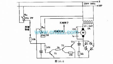
In the figure, potentiometer Rp2's sliding contact-point axis is connected with the antenna axis. Only when the Rp1 and Rp2 point at the same position, the transistors will not turn on, and the rectifier bridge will close, there is no voltage on the motor, so the antenna is not moving, Otherwise, the antenna or motor will synchronously turn with the given potentiometer. (View)
View full Circuit Diagram | Comments | Reading(2611)
SG201 leakage protection IC diagram
Published:2011/5/9 2:23:00 Author:Ecco | Keyword: leakage protection , IC


SG201 is the specific leakage protection integrated circuit, which is widely used in a variety of leakage protection. 1. Features of functionsSG201 IC includes voltage regulator circuit, reference voltage circuit, the differential amplifier circuit, level judging and shaping output circuit, the internal block circuit diagram is shown as the chart. 2. Pin functions and data SG201 integrated circuit uses 8-pin dual in-line package, the pin functions and data are listed in table. Operating current is 1.8 ~ 2.5mA, so the static power consumption is low. 3. The typical application circuit The typical application circuit of SG201 IC leakage protection circuit is shown in Figure 1.
(View)
View full Circuit Diagram | Comments | Reading(887)
RY901 fan monolithic microcomputer integrated circuit diagram
Published:2011/5/9 3:22:00 Author:Ecco | Keyword: fan , monolithic , microcomputer, integrated circuit


RY901 is the fan monolithic microcomputer integrated circuit, which is widely used in processing control fan circuit. KY901 IC uses 16-pin dual in-line plastic package, the pin functions and data are listed in Table, the typical application circuit is shown as the chart.
(View)
View full Circuit Diagram | Comments | Reading(1103)
| Pages:1923/2234 At 2019211922192319241925192619271928192919301931193219331934193519361937193819391940Under 20 |
Circuit Categories
power supply circuit
Amplifier Circuit
Basic Circuit
LED and Light Circuit
Sensor Circuit
Signal Processing
Electrical Equipment Circuit
Control Circuit
Remote Control Circuit
A/D-D/A Converter Circuit
Audio Circuit
Measuring and Test Circuit
Communication Circuit
Computer-Related Circuit
555 Circuit
Automotive Circuit
Repairing Circuit