
Signal Processing
Index 55
Complementary tube pulse circuit principle and applied circuit diagram
Published:2011/9/9 7:51:00 Author:Vicky | Keyword: complementary tube pulse circuit

(picture1)
Complementary tube bistable state circuit is shown in picture1(a). When the power is on, if no triggering signal works, the two tubes stop working and the state is in a stable state because the collector current is extramely small, and the end voltage of RC1, and Rc2 (bias current provided to the two tubes) is also very small.
When the trigger pulse is working, suppose that BG1 becomes amplified from static, and leads to the process of avalanche-type positive feedback. Soon the two tubes become saturate, and are in another stable state. Capacitance C1 is speed-up capacitor. From picture1(b), we can see that uc1 goes down to zero sharply from Ec, while Uc2 zooms up to Ec from zero. (View)
View full Circuit Diagram | Comments | Reading(1000)
Schematic and applied circuit diagram of tunnel diode pulse circuit
Published:2011/9/9 7:56:00 Author:Vicky | Keyword: tunnel diode pulse circuit

Volt-ampere characteristics and parameter of tunnel diode
Volt-ampere characteristics of tunnel diode (see picture a) is a S pattern curve. The highest current point P in the curve is called the peak; the lowest current point V is called valley point. The main parameters of the tunnel diode are:
(1) Peak point voltage Up is about dozens of millivolt; valley point voltage Uv is about hundreds of millivolt.
(2) Peak point current Ipi is about several milliampere; valley point voltage Iv is about hundreds of microampere.
(3) Proportion of peak point current and valley point current is about 5-6; the higher, the better.
(4) Valley point capacitance Cv of from several microfarad to dozens of microfarad, and the lower, the better; 2BS4A made in China: Up=80 millivolt, Ip = 4 milliampere, valley point current proportion ≥5, Cv = 10~15 microfarad, Uv = 280 millivolt. (View)
View full Circuit Diagram | Comments | Reading(1328)
the relaxation oscillation circuit with 300MHZ frequency modulation
Published:2011/9/8 6:16:00 Author:Ariel Wang | Keyword: relaxation oscillation , 300MHZ, frequency modulation
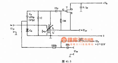
The oscillation circuit signals come from UA2 or UA1.LK is one turn within 300MHZ.L' is about 10% of L's turns.You can do frequency fine adjustment to UD using varactor CD.And you can do frequency modulation to UNF.If you want to choose the capacitor CS,you can refer to the frequency range and the varactor based on the frequency offset required.The capacitor C in oscillating circuit can be chosen as the way above.
(View)
View full Circuit Diagram | Comments | Reading(898)
Ladder wave generation circuit composed of the 74HC193
Published:2011/8/24 21:30:00 Author:Christina | Keyword: Ladder wave, generation circuit

The ladder wave generation circuit which is composed of the 74HC193 is as shown in the figure. In this circuit, the 74HC193 is the 4-bit binary counter, we can connect the R-2R trapezoidal resistance network at the output port of it to form the 4-bit D/A converter. The number 15 stage voltage is the value of the trapezoidal network, 5Vxl5/16=4.6875V, the voltage of every stage is 312.5mV. In order to make the maximum output voltage is 10V, we use the A1 to amplify it 2 times. When the stepped voltage of every stage is not suitable, we can divide it at the output port.
(View)
View full Circuit Diagram | Comments | Reading(3314)
Simple flashing annunciator circuit diagram
Published:2011/8/30 20:59:00 Author:Lucas | Keyword: Simple flashing annunciator
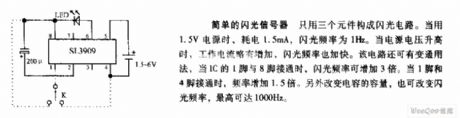
It only uses three components to form the flashing circuit. When it uses 1.5V supply, it consumes 1.5mA, and the flashing frequency is 1Hz. When the supply voltage rises, the operating current increases slightly, and the flashing frequency is accelerated. The circuit also has alternative uses, when the pin 1 of IC is connected to pin 8, the flashing frequency is increased 3 times. When pin 1 is connected pin 4, the frequency is increased 1.5 times. Also changing the capacitor also can change the flashing rate to 1000Hz.
(View)
View full Circuit Diagram | Comments | Reading(1069)
Colpitts oscillator circuit diagram
Published:2011/8/18 1:22:00 Author:Jessie | Keyword: Colpitts oscillator
View full Circuit Diagram | Comments | Reading(1428)
High-frequency high-voltage oscillator(DC voltage convertor) circuit diagram
Published:2011/8/18 1:23:00 Author:Jessie | Keyword: High-frequency high-voltage oscillator, DC voltage convertor

View full Circuit Diagram | Comments | Reading(1286)
Electronic voltage regulated electromagnetic vibration circuit diagram
Published:2011/8/18 1:29:00 Author:Jessie | Keyword: Electronic voltage regulated, electromagnetic vibration

View full Circuit Diagram | Comments | Reading(1078)
Complementary tube free running multivibrator circuit diagram
Published:2011/8/18 1:47:00 Author:Jessie | Keyword: Complementary tube, free running, multivibrator

View full Circuit Diagram | Comments | Reading(980)
Multiple unit tube RC bridge oscillation circuit diagram
Published:2011/8/18 2:12:00 Author:Jessie | Keyword: multiple unit tube, bridge, oscillation

View full Circuit Diagram | Comments | Reading(925)
Common emitter inductance feedback oscillation circuit diagram
Published:2011/8/18 2:14:00 Author:Jessie | Keyword: common emitter, inductance feedback oscillation

View full Circuit Diagram | Comments | Reading(808)
The multi-function ultrasonic humidifier circuit
Published:2011/8/23 22:08:00 Author:Borg | Keyword: multi-function, ultrasonic humidifier
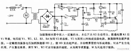
When there is some water in the humidifier, the water level switch K2 is pulling in automatically. When the power supply K1 is put through, the voltage is added on the base electrode of V2 by V1, W2, L2, R3 and R4, V2 forms the oscillator with its external elements, the oscillator frequency is in ultrasonic waveband. When the oscillating voltage of certain amplitude is added on the converter HD, HD will generate the ultrasonic wave, and is will form resonance in the fog tube, which has some effect on water and fog is generated. By adjusting W1 and W2, the amplitudes of W1 and W2 can be changed, so the fog content is adjusted.
(View)
View full Circuit Diagram | Comments | Reading(4536)
The electronic frostbite instrument circuit
Published:2011/8/23 22:11:00 Author:Borg | Keyword: electronic, frostbite instrument
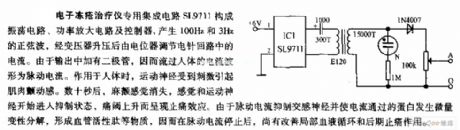
The electronic frostbite instrument special integrated circuit SL9711 forms the oscillating circuit, power amplifier circuit and controller, it generates the sine waves of 10Hz and 3Hz, after it is boosted by the transformer, the current is adjusted by the potentiometer. As there are diodes in the output, so the shape of the current running through human body is the impulse current. When it is working on the human body, the motor nerves cause the muscle shake due to the stimulation. In several seconds, the palsy feel is gone, the feeling and motor nerves are starting to turn into the impedance state, the anti-pain effect is appearing as the pain valve is rising up.
(View)
View full Circuit Diagram | Comments | Reading(694)
Function generator circuit composed of the ICL8038
Published:2011/8/24 20:49:00 Author:Christina | Keyword: Function, generator
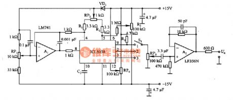
The function generator circuit which is composed of the ICL8038 is as shown in the figure. The ICL8038 is composed of the charging and discharging current source, the comparator, the bridge and the broken line approximation circuit. This circuit can be used as the operating mode of the voltage-controlled oscillator, we add the A1 to improve the linearity of the control voltage. The oscillation frequency is decided by the control voltage (the output voltage of RP1), the resistance value of RP2, the R1, R2 and R3. The output impedance of ICL8038 is decided by the R3, when there is the triangular wave, the resistance value is 200Ω. Because the waveform distortion is large, so it can not output the sine wave in the high impedance state, so we add the buffer amplifier A2.
(View)
View full Circuit Diagram | Comments | Reading(7389)
Sawtooth wave generator circuit composed of the CD4040
Published:2011/8/23 22:37:00 Author: | Keyword: Sawtooth wave, generator circuit
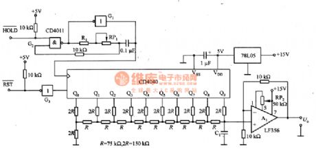
The Sawtooth wave generator circuit composed of the CD4040 is as shown in the figure. This circuit is composed of the clock oscillator, the CD4040 10-bit counter, the R-2R ladder network, the 78L05 reference voltage generator, the A1 buffer amplifier.
The clock oscillator uses the astable multivibrator which is composed of the gate circuit G1, and it can be used in the low frequency oscillation. The CD4040 is the binary counter, you can produce the high precision sawtooth wave by increasing the number of bits. If the VDD terminal voltage of the CD4040 is not stable, the amplitude of the sawtooth wave will change, so we need to use the 78L05 three-port stabilizer to stabilize the voltage.
(View)
View full Circuit Diagram | Comments | Reading(5501)
Constant amplitude sawtooth wave generating circuit composed of the μA741
Published:2011/8/25 20:59:00 Author:TaoXi | Keyword: Constant amplitude, sawtooth wave, generating circuit
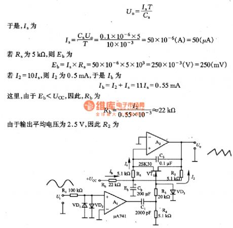
The constant amplitude sawtooth wave generating circuit composed of the μA741 is as shown in the figure. This circuit changes the input signal of the external oscillator into the square wave signal, and this signal changes into the pulse signal that can drive the VT1 grid electrode through RC(R4, C1) differential, the VT1 makes the integral capacitance Cs in the short-circuit state periodically, A2 outputs the constant amplitude sawtooth wave with the cycle of T.
Now I briefly explain the method of setting circuit parameters. If the frequency of the external input oscillation signal is 50HZ (the corresponding period T is lOms), the VT1 conduction resistor is 2OOΩ.
(View)
View full Circuit Diagram | Comments | Reading(1248)
Burst sound generator circuit composed of the SN7473
Published:2011/8/25 21:47:00 Author:TaoXi | Keyword: Burst sound, generator circuit
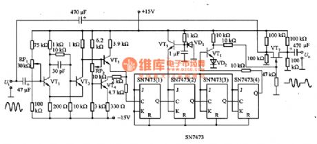
The burst sound generator circuit composed of the SN7473 is as shown in the figure. When the sine wave is changing into the burst sonic, it needs the wveform shaping circuit, the frequency dividing circuit and the switching circuit. As the figure 6-64 shows, the waveform shaping circuit uses the schmitt circuit; the frequency dividing circuit uses the T trigger; the switching circuit uses the FET tube. The SN7473 is the frequency dividing circuit, when the Q outputs the high level, the VT6 conducts, the grid electrode of VT7 outputs the low level and cuts off to change into the high impedance and output the U. When the Q outputs the low level, the VT6 cuts off, the VT7 conducts to output the U.
(View)
View full Circuit Diagram | Comments | Reading(1360)
Ramp function generator circuit composed of the TA7507
Published:2011/8/25 22:23:00 Author:TaoXi | Keyword: Ramp, function, generator
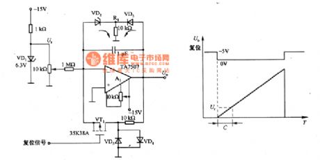
The ramp function generator circuit composed of the TA7507 is as shown in the figure. This circuit is designed as one kind of Mueller integral circuit, and it changes into the ramp function generator circuit by adding some related components. In this circuit, the VT1 is the N channel MOSFET tube (0V cut-off and +5V conduction), the vd4 and vd5 clamp the drain voltage of VT1 at 0V. When the output voltage increases, it can prevent the VT1 to be damaged.
When the VT1 is in the cut-off state, the A1 integrates the input benchmark voltage U, so the circuit outputs the ramp waveform. In the circuit, A1 uses the A7507, it is one kind of FET input type operational amplifier.
(View)
View full Circuit Diagram | Comments | Reading(2440)
The ladder wave generator circuit composed of the SN74163
Published:2011/8/26 2:14:00 Author:TaoXi | Keyword: ladder wave, generator
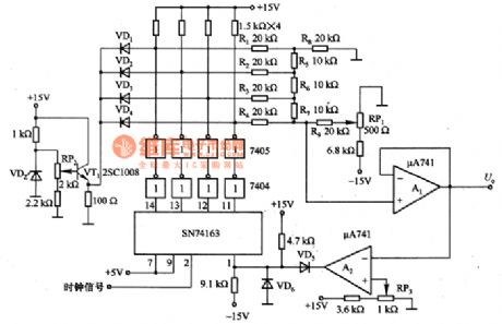
The ladder wave generator circuit composed of the SN74163 is as shown in the figure. In this circuit, the SN74163 is the synchronous counter which is the same as the clock, it can choose the frequency dividing ratio, so this device is very convenient. The VDZ and VT1 are the reference power supply that can supply the reference voltage to the D/A converter. The R1~R9 are the ladder-shaped D/A converter, it changes the input digital quantity into the analog voltage. The 7404 and 7405 are the buffer; A2 is the comparator; A1 is the outputbuffer, it outputs the step-wave voltage. RP1 is the step 1 regulation voltage; RP2 can be used to adjust the maximum voltage of the step; RP3 can be used to adjust the number of the step.
(View)
View full Circuit Diagram | Comments | Reading(1227)
Pulse generator circuit composed of 74121
Published:2011/8/26 2:27:00 Author:TaoXi | Keyword: Pulse, generator
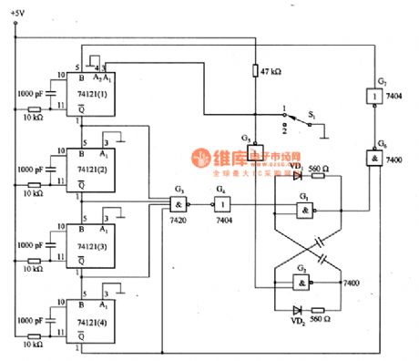
The pulse generator circuit composed of 74121 is as shown in the figure. In this circuit, the 74121(1)~74121(4) are the monostable multivibrator, the σ of the 74121(1) adds to the B port of the 74121(2), similarly, the σ of the 74121(2) adds to the B port of the 74121(3). The σ of the 74121(4) gets through the G6 and G7 gate circuits to go back to the input B of the 74121(1). When the power is connected or there is the external noise, the 74121(1)~74121(4) will produce the oscillation, the σ is in the high level stable state, and the G3 gate circuit detects the σ output of the monostable multivibrators. The G3 output signal is inversed by G4 to control the G1 and G2 to form the oscillation of the unsteady many harmonic oscillator.
(View)
View full Circuit Diagram | Comments | Reading(2315)
| Pages:55/195 At 204142434445464748495051525354555657585960Under 20 |
Circuit Categories
power supply circuit
Amplifier Circuit
Basic Circuit
LED and Light Circuit
Sensor Circuit
Signal Processing
Electrical Equipment Circuit
Control Circuit
Remote Control Circuit
A/D-D/A Converter Circuit
Audio Circuit
Measuring and Test Circuit
Communication Circuit
Computer-Related Circuit
555 Circuit
Automotive Circuit
Repairing Circuit