
Signal Processing
Index 54
The 74 series digital circuit of 74123 74L123 double monostable multivibrator
Published:2011/9/18 21:07:00 Author:Ecco | Keyword: The 74 series, digital circuit, double monostable multivibrator


Capacitance. To improve the precision and repeatability of the pulse width, it could connect a resistance between REXT/CEXT and VCC, and open for RINT. In order to get the variable pulse width, it could connect a variable resistance between RINT and VCC.
74123, 74L123, 74LS123, 74HC123 double monostable multivibrator (View)
View full Circuit Diagram | Comments | Reading(2424)
The 74 series digital circuit of 74121 74L121 monostable multivibrator
Published:2011/9/18 21:06:00 Author:Ecco | Keyword: 74 series, digital circuit, monostable multivibrator


To improve the precision and repeatability of the pulse width, it could connect a resistance between REXT/CEXT and VCC, and open for RINT.
To improve pulse width, it could connect atiming resistance betweenREXT/CEXT and CEXT. (View)
View full Circuit Diagram | Comments | Reading(2119)
Two Wien Bridge low-frequency signal generators for self-made
Published:2011/8/2 1:11:00 Author:Ecco | Keyword: Wien Bridge, low-frequency , signal generator , self-made

Low frequency signal generator is the common equipment for electronic production debugging, maintenance, here are two circuits, the performance are very good. The two 100kΩ resistors in figure and two 1600pF capacitors determine the oscillation frequency of RC series-parallel selective circuit, it is calculated as f = 1 ÷ (6.28 × R × C). If the unit of R uses kΩ, the unit of C uses μF, the unit of f is kHz, so changing the value of R and C according to the calculation, then you can get a different oscillation frequency. The frequency of RC circuit diagram is l000Hz. It should be noted, the value of resistors and capacitors in two series-parallel network must be the same. This circuit has the advantage of easy startup, good wave and reliable work, it is often called the Wien Bridge oscillator circuit.
(View)
View full Circuit Diagram | Comments | Reading(863)
The Colpitts oscillator
Published:2011/9/18 20:55:00 Author:Ecco | Keyword: colpitts , oscillator

Figure shows the Colpitts oscillator circuit. It has a base frequency crystal, and the frequency is 1499 kHz, crystal SJT is connected to the both ends of capacitor C2, C3. Emitter divider resistor R2, R3 provide basic feedback signal, the feedback voltage is controlled by the capacitive dividers C2, C3. SJT crystal provides l499kHz sine wave signal for the base of the transistor VT after working. And it is output by VT emitter output VT.
Resistors R1 provides a 18V step-down voltage for a proper bias voltage of VT, appropriately adjusting resistor R1 could make Colpitts oscillator work in the soft excitation state. Resistor R4, capacitor C5 is post-coupling circuit. Regulating capacitor C1 can fine-tune the oscillator working frequency. Adjusting potentiometer RP can change the oscillation signal output level. Selecting components: capacitors Cl, 5 ~ 20p, C2 to 51p, C3, C6 to 100p, C4 to 15p, C5 is 100μ/32V. Resistor Rl is 62kΩ, R2 is 300Ω, R3 is 2.4kΩ, R4 is 360Ω, 1/2W, R5 is 15kΩ. Potentiometer RP is 4.7kΩ. Transistor VT is 3DGl20C, 65 ≤ β ≤ 115. Zener diode VD uses 2CW58. crystal SJT uses JA5B-1499Hz.
(View)
View full Circuit Diagram | Comments | Reading(2642)
Fixed-amplitude RC phaser oscillator circuit diagram
Published:2011/9/2 1:34:00 Author:Ecco | Keyword: Fixed-amplitude RC, phaser oscillator

View full Circuit Diagram | Comments | Reading(1105)
Low-cost second signal oscillator circuit diagram
Published:2011/9/9 2:34:00 Author:Ecco | Keyword: second signal oscillator

View full Circuit Diagram | Comments | Reading(722)
Three-phase output oscillator circuit diagram
Published:2011/9/2 1:36:00 Author:Ecco | Keyword: Three-phase output , oscillator

View full Circuit Diagram | Comments | Reading(1333)
Sine wave generation schematic circuit diagram
Published:2011/9/9 1:57:00 Author:Ecco | Keyword: Sine wave generation

View full Circuit Diagram | Comments | Reading(2161)
Oscillator connection circuit diagram
Published:2011/9/1 1:55:00 Author:Ecco | Keyword: Oscillator connection

View full Circuit Diagram | Comments | Reading(674)
Multi-waveform signal generator circuit diagram
Published:2011/9/9 1:49:00 Author:Ecco | Keyword: Multi-waveform signal generator

View full Circuit Diagram | Comments | Reading(1791)
CD4046 FM signal generator circuit diagram
Published:2011/9/9 1:48:00 Author:Ecco | Keyword: FM signal generator
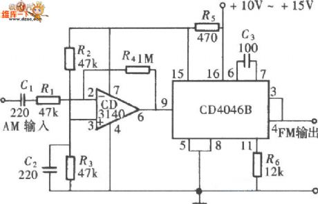
View full Circuit Diagram | Comments | Reading(4163)
CD4046 square-wave generator circuit diagram
Published:2011/9/9 1:37:00 Author:Ecco | Keyword: square-wave generator
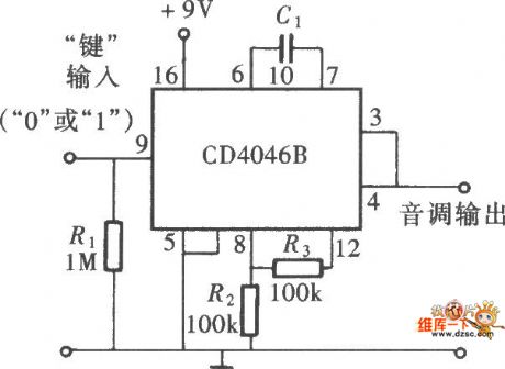
View full Circuit Diagram | Comments | Reading(1719)
Elliptic filter circuit diagram
Published:2011/9/14 2:07:00 Author:Ecco | Keyword: Elliptic filter
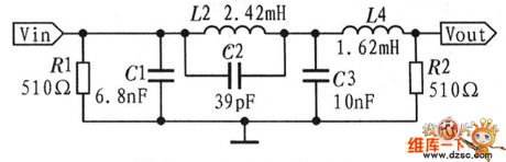
View full Circuit Diagram | Comments | Reading(2096)
MAX262 Programmable filter circuit
Published:2011/9/13 21:15:00 Author:Ecco | Keyword: Programmable filter
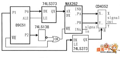
Programmable filter is mainly achieved by the MAX262. MAX262 achieves programmable filter from filter parameters programmed by the SPI bus, and the center frequency and quality factor are 64, 128-level programming adjustable, the circuit is shown as the chart.
(View)
View full Circuit Diagram | Comments | Reading(857)
Broadband pulse generator circuit diagram with independent adjustable duty cycle
Published:2011/9/14 9:14:00 Author:nelly | Keyword: Broadband pulse generator, adjustable duty cycle
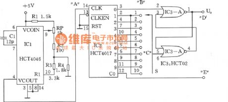
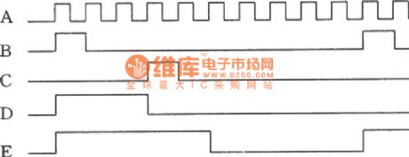
As shown in the figure, this circuit can provide adjustable square wave and rectangular wave generator 1.2KHz~2.7KHz work frequency, 10~90% duty cycle. The frequency comes form the voltage controlled oscillator and correlative components. The 1.2KHz~2.7KHz oscillation frequency is adjusted by potentiometer RP. The counter IC2 provides set pulse which form Q0 output to SR trigger IC3, the corresponding reset pulse is decided by Q1~Q9 output select switch S. The output frequency is 1/10 of IC2's input, the square wave is obtained form carry output C .
(View)
View full Circuit Diagram | Comments | Reading(1464)
Low power consumption wien bridge oscillator circuit diagram composed of MC1454
Published:2011/9/14 9:15:00 Author:nelly | Keyword: wien bridge oscillator
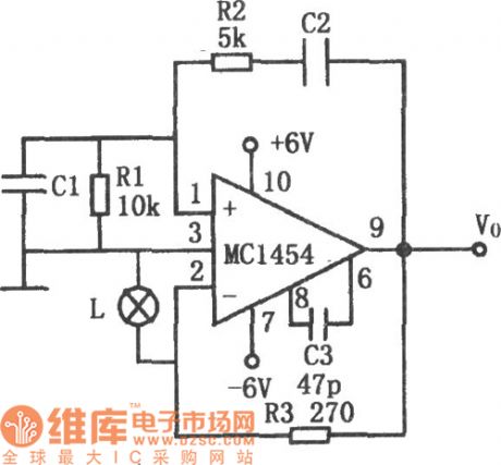
As shown in the figure, it is a low power consumption wien bridge oscillator circuit. When it drives low impedance and large capacitance loads, the distortion is small. The used operational amplifier can drive 8~10Ω loads, it can provide 2~4V peak value outout voltage, the frequency ranges from 1Hz to 100KHz, the distortion is lower than 0.5%. The automatic gain control is realized by bulb L, because the bulb's resistance changes in relation to the output voltage. The negative feedback circuit is composed of resistance R3, then it can determine the output signal amplitude.
(View)
View full Circuit Diagram | Comments | Reading(1187)
Integrated Circuit of High-fidelity Dual Track Amplifier TDA2616
Published:2011/9/12 23:57:00 Author:Zoey | Keyword: Integrated Circuit, High-fidelity, Dual Track, Amplifier
1.Circuit Diagram and pin function of TDA2611A
TDA2616 is used as power amplifiers in TV sounders, compound sounders and active sounders.
There are two identical audio frequency amplified circuits in TDA2616 integrated block. Its integrated block interior circuit and dual power supply circuit have been presented in the picture. In this IC, pin 9 is single inline encapsulation, pin function and statistics have been presented in the chart.
2 Main parameters of TDA2616
(1) Dual power supply. If Vcc=±16V, R(l)=8Ω,THD=0.5%,Po=12W. If THD=10%,Po=15W.
(2)Single power supply. If Vcc=24V, THD=10%, if R(l)=4Ω, Po=14W.
3 Typically-applied Circuit of TDA 2616. As shown in picture, they refer to TDA dual power supply circuit and integrated block single power supply circuit respectively.
4 Malfunction Examination and repair alert
Whether it is a single supply or dual power supply, when there is a silent failure, we should firstfigure ourifthe squelch circuit isin the wrong starting state. We canjudge the statebycutting off pin 2.
(View)
View full Circuit Diagram | Comments | Reading(862)
The voltage-controlled oscillator circuit with high output amplitude stability
Published:2011/9/12 21:52:00 Author:TaoXi | Keyword: Voltage-controlled, oscillator, high, output amplitude, stability

The voltage-controlled oscillator circuit with high output amplitude stability is as shown in the figure. In this circuit, the VT2 controls the collector electrode current of VT1, so the oscillation amplitude of VT1 is very stable. The output signal of VT4 is detected by VD2 to change into the DC signal, it is the automatic gain control working state, so you can make the DC voltage keep constant. The midpoint voltage of RP1 is -0.6V, the current of R1 and R2 can keep the equal, so we can make the output amplitude keep in a constant value. The oscillation frequency is decided by the L1, C2, the capacitance of VD1 and the distributed capacitance.
(View)
View full Circuit Diagram | Comments | Reading(1016)
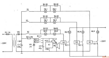
Ward Caller Five
Published:2011/8/12 1:43:00 Author:Felicity | Keyword: Ward Caller
Work of the circuit
The circuit consists of power circuit, triggers control circuit and the acousto-optic call circuit. (It is showed in picture 9-88.)
Power circuit consists of fuse FU, power transformer T, rectifier diode VD, filter capacitor Cl, limiting resistor R7 and zener diode VS.
Triggers control circuit consists of Sl-S3 (ward bedside switch), resistors Rl-R6 and light HLl-H calendar and relay Kl-K3.
The acousto-optic call circuit consists of light HU-HLg, KI-K3 normally open contact, capacitor C2, music integrated circuit IC, transistor V, and the speaker BL.
This ward caller consists of power supply circuit ,trigger-control circuit and acousto-optic calling circuit.
When S1-S3 are not pressed, HL1-HL9 are all off and BL is noiseless. When one of S1-S3 is pressed, the relay in this branch closes, and the indicator is on. At the same time IC is power on and the music electrical signal output by O/P is amplified by V to drive BL to send out music sound. For example while S2 is pressed, HL3 and HL4 is on. Then K2 closes, and the normally open contacts K2-1 and K2-2 are switched on to make HL8A on, and BL sends out music sound.
(View)
View full Circuit Diagram | Comments | Reading(781)
Schematic and applied circuit diagram of pulse circuit composed of photoelectric coupler
Published:2011/9/9 7:54:00 Author:Vicky | Keyword: Schematic and applied circuit diagram, pulse circuit composed of photoelectric coupler

picture1
picture2
When Ec is just on in picture 1(a), Up increases when C is charging. When UF≈1, luminous diode and then the triode become saturate, and output Uo≈Ec.
When triode becomes saturate, C discharges (through two route: C→F→E1→Er and C→RF→+Ec→R ). Uo becomes lower. The diode stops when c discharges to a certain degree. The triode stops subsequently after moving all the memory electric charge, and uo becomes zero. Power Ec charges C again after triode stops, and the above process repeats again. Thus the peak output wave is obtained, and the cycle is (when RF》Re ): T=C(RF+Re)In2 (View)
View full Circuit Diagram | Comments | Reading(992)
| Pages:54/195 At 204142434445464748495051525354555657585960Under 20 |
Circuit Categories
power supply circuit
Amplifier Circuit
Basic Circuit
LED and Light Circuit
Sensor Circuit
Signal Processing
Electrical Equipment Circuit
Control Circuit
Remote Control Circuit
A/D-D/A Converter Circuit
Audio Circuit
Measuring and Test Circuit
Communication Circuit
Computer-Related Circuit
555 Circuit
Automotive Circuit
Repairing Circuit