
Oscillator Circuit
Index 51
Two-Phase Output Sine Wave Oscillator Circuit
Published:2011/4/21 20:26:00 Author:Robert | Keyword: Two-Phase, Sine Wave, Oscillator

Two-Phase Output Sine Wave Oscillator Circuit is shown below:
(View)
View full Circuit Diagram | Comments | Reading(1594)
Very Cool Sine Wave Generation Circuit
Published:2011/4/21 9:37:00 Author:Robert | Keyword: Sine Wave, Generation
Very Cool Sine Wave Generation Circuit is shown as below:
(View)
View full Circuit Diagram | Comments | Reading(825)
Stable Sine Wave Oscillator Circuit
Published:2011/4/21 9:49:00 Author:Robert | Keyword: Sine Wave, Oscillator
Stable Sine Wave Oscillator Circuit is shown below:
(View)
View full Circuit Diagram | Comments | Reading(787)
The multivibrator composed of D flip-flop
Published:2011/4/14 2:38:00 Author:Ecco | Keyword: multivibrator , D flip-flop
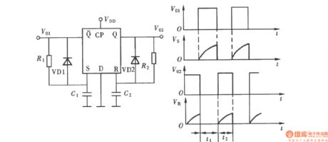
T0 connect theQ output terminal of D flip-flopto RC components toform a monostable trigger. The non-output terminal of Q connects to a group of RC components, they will make up a non-steady-state circuit, and it's a multivibrator. The composition is shown as the chart:
(View)
View full Circuit Diagram | Comments | Reading(1362)
Dual D flip-flop VCO
Published:2011/4/18 20:14:00 Author:Ecco | Keyword: Dual D, flip-flop , VCO
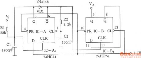
The chart shows the dual D flip-flop VCO. Circuit outputs a 50% duty cycle square wave signal, while the consumption of current is very low. When the input voltage is 5 ~ 12V, the output frequency ranges from 20 ~ 70kHz. First assuming the initial state of IC-A is Q = low level. At this time, VDl turns off, Vi charges to Cl through Rl. When the voltage on Cl reaches a certain voltage level, IC-A is forced to flip, its Q output is in high level, Cl discharges through VDl. At the same time, the CL input of IC-A will be transformed into low level, IC-A is forced back to Q = low level. The delay effect of R2 and C2 discharges the electricity of C1 before the IC-A returning to the state of Q = low level. The narrow pulse current of IC-A triggers IC-B, it produces a 50% duty cycle output pulse signal.
(View)
View full Circuit Diagram | Comments | Reading(1496)
Variable quartz crystal oscillator (VXO) circuit
Published:2011/4/20 1:19:00 Author:Ecco | Keyword: Variable , quartz crystal , oscillator , VXO

The chart shows two typical VXO circuits, in fact they arePierce circuits,the difference is theconnection.
(View)
View full Circuit Diagram | Comments | Reading(2502)
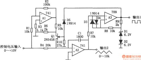
First-order active phase shift oscillator(F007)
Published:2011/4/20 2:32:00 Author:Ecco | Keyword: First-order, active, phase shift , oscillator

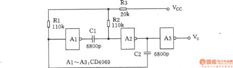
The chart shows the first-order active phase shift oscillator. In the circuit, A1 and A2 form the first order active phase shifter, and they form loops with A3. A3 is the inverting proportion amplifier, it has the effect of primary amplification, the gain adjustment is -l, the phase shift is π. D1, D2 are the regulator 2DW7C, they play the role of steady increase. According the conditions required for the oscillation, transmission coefficient | β | of the first order active phase shifter is 1. When the total phase shift is π, the circuit can oscillate, the oscillation frequency: f0 = 1/2πRC.
(View)
View full Circuit Diagram | Comments | Reading(739)
High-performance quadrature sine wave oscillator
Published:2011/4/20 2:14:00 Author:Ecco | Keyword: High-performance , quadrature , sine wave , oscillator

Many RC oscillators use advanced circuit in phase shift unit. It uses a voltage feedback amplifier, of which the gain will get a sharp decline in a higher frequency and stop oscillation before reaching the desired frequency. That is the reason why voltage feedback amplifier has poor phase characteristics. The RC oscillator composed of high-frequency IC HA5025 with four current-feedback amplifiers will produce four sine waves. The circuit is shown as the chart. CD74AC00 has four NAND gates, when the threshold is bias, four independent amplifiers of HA5025 produce four sine waves, sine wave AC coupled into the input which is used as a sine / square wave converter.
(View)
View full Circuit Diagram | Comments | Reading(2663)
Single-junction transistor sine wave oscillator
Published:2011/4/20 2:22:00 Author:Ecco | Keyword: Single-junction, transistor , sine wave , oscillator

The single-junction transistor is often used in sawtooth generator and pulse generator, but it may also constitute a simple sine wave generator circuit. As an scillator circuit with discrete components, it uses few components. Circuit is shown as the chart. And comparing with ordinary unijunction relaxation oscillator circuit, it adds a LC tuned circuit to the second base, the tuned circuit generates sinusoidal oscillation depended on the driving of unijunction excitation current pulse. Adjusting resistor Rl can control the size of the current pulse, sine wave can be obtained at B2. According to the parameters of figure, the oscillation frequency is 3750Hz, the peak value of output voltage peak is 2V.
(View)
View full Circuit Diagram | Comments | Reading(3843)
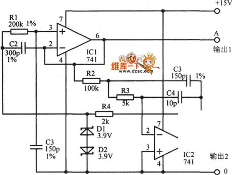
1kHz sine wave oscillator(741)
Published:2011/4/20 2:42:00 Author:Ecco | Keyword: 1kHz , sine wave, oscillator

The circuit shown in the chart is 1kHz sine wave oscillator circuit. Basing on the double-T circuit, the circuit using 741ordinary operational amplifier to produce 1000Hz sine wave output. Adjusting 100kΩ potentiometer will make circuit start oscillation, the oscillation frequency is determined by R1 and R2, and under normal circumstances, the value of two resistors is equal, the oscillation frequency is in inversely proportion with the resistance. Usually, the resistance is chosen between 4.7 ~ 18Ω, when the resistance of R1 and R2 is determined, the capacitor size could be selected according to need. In the figure, the resistor value choses 13Ω, capacitance is 0.01/μF.
(View)
View full Circuit Diagram | Comments | Reading(12040)
CMOS Gate voltage-controlled oscillator
Published:2011/4/14 2:33:00 Author:Ecco | Keyword: CMOS, Gate , voltage-controlled oscillator
In the circuit that as shown in the chart, the free-running multivibrator is composed of two NOT gates of A1 and A2. With the changing of external control voltage Vcc, the circuit oscillation frequency will change. When the value of VCC is near the threshold of gate,it has the least impact on charging and discharging of RC. The greater deviation between VCC and threshold of gate, the capacitor charges and discharges faster, so the oscillation frequency of the circuit is more resistant.
(View)
View full Circuit Diagram | Comments | Reading(736)
The self-excited multivibrator composed of CC4093
Published:2011/4/19 6:47:00 Author:Ecco | Keyword: self-excited , multivibrator
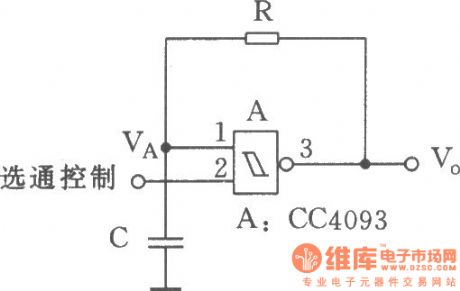
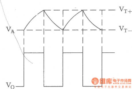
It needs a resistance and a capacitor connecting externally when forming a multivibrator by Schmidt trigger. The circuit is used to the low frequency vibration source which has lower demand for accuracy, and the vibration is controlled. The circuit in the figure is a self-excited much harmonic oscillator composed of four 2 input Schmidt trigger.
(View)
View full Circuit Diagram | Comments | Reading(551)
Keyer oscillator
Published:2011/4/19 3:02:00 Author:Ecco | Keyword: keyer, oscillator
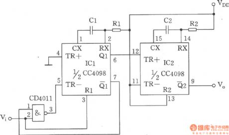
The chart shows a keyer oscillator composed of double monostable triggerCC4098, four 2 input NAND Gate CC4011. The circuit is a keyer oscillator with adjustable keying frequency and duty cycleformed by the monostable trigger, it ismainly usedfor the low frequency signal generatorrequiring less precision.
(View)
View full Circuit Diagram | Comments | Reading(12)
Multi-output crystal oscillator
Published:2011/4/19 1:44:00 Author:Ecco | Keyword: Multi-output , crystal, oscillator
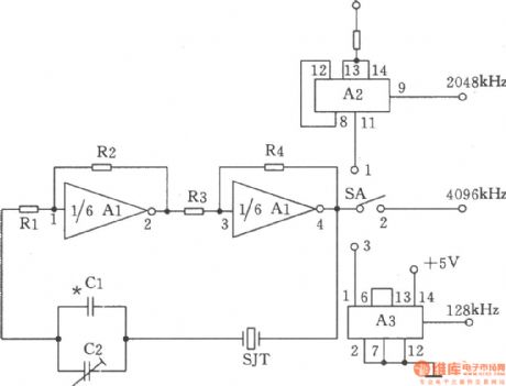
The chart shows the multi-output crystal oscillator. It is mainly composed of three gates of A1, four resistors, two capacitors and a crystal. Rl ~ R4 bias two inverters in the linear range, and they are connected between the pin 4 and pin1 of A1 by the crystal SJT, and they are used to provide feedback loop. It only produces frequency on the fundamental frequency of crystal. The selection of components: capacitor Cl is 15p (vernier capacitor). Resistors Rl, R3 are 220Ω, R2 is 560Ω, R4 is 1.8kΩ, R5 is 1kΩ, the nominal power is l/8W. IC Al is 7404, A2 is the 74LS74, A3 is the 74LS393. Crystal SJT is SW60A-4096kHz. Switch SA is KNX (1 × 3).
(View)
View full Circuit Diagram | Comments | Reading(719)
Adjustable duty cycle multivibrator composed of 555
Published:2011/4/19 1:08:00 Author:Ecco | Keyword: Adjustable, duty cycle , 555, multivibrator
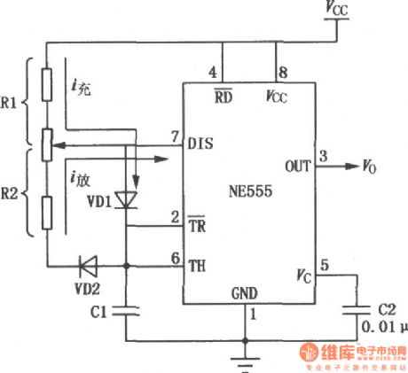
View full Circuit Diagram | Comments | Reading(1069)
Linear CMOS oscillator
Published:2011/4/18 22:26:00 Author:Ecco | Keyword: Linear, CMOS , oscillator
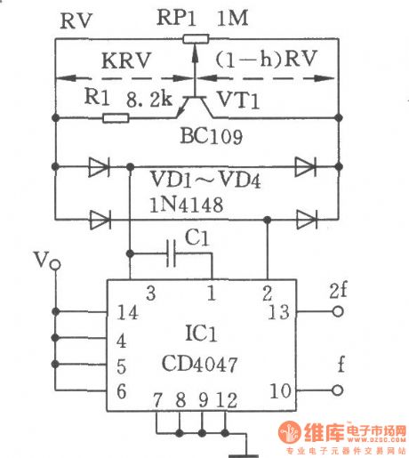
The linear CMOS oscillator circuit is shown as the chart. Just using a potentiometer RPl to make the CD4047 CMOS oscillator frequency be adjusted in the range of 1:100, and then accessing a transistor used as a variable resistor, and that is a regulator circuit with a line relationship to frequency. The emitter resistor R1 of VTl and base voltage could set the collector current. The bridge composed of diode VDl ~ VD4 ensures the symmetry work in positive and negative half-cycle.
(View)
View full Circuit Diagram | Comments | Reading(1187)
Voltage-controlled sinusoidal oscillator composed of MC1046B
Published:2011/4/18 20:10:00 Author:Ecco | Keyword: Voltage-controlled , sinusoidal , oscillator
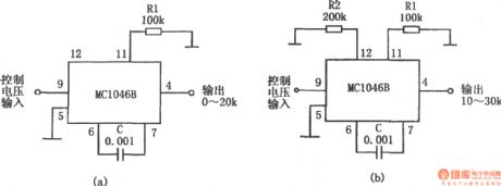
The voltage-controlled sinusoidal oscillator circuit is shown in the chart. It is composed of MC1046B. When the controlling input voltage is 0 ~ 5V, the outputcan get the sine signal withfrequencyfrom 0 ~ 20kHz.The frequency range is decided by the resistor R1 and capacitor C, changing the resistors and capacitorscould change the oscillation frequency. If the external resistor R2 connects topin 12 , oscillation frequency range could be changed. If you choose R2 = 2R1, the oscillation frequency becomes 10 ~ 30kHz.
(View)
View full Circuit Diagram | Comments | Reading(1057)
The voltage-controlled oscillator with triangular wave and square wave output
Published:2011/4/18 1:59:00 Author:Ecco | Keyword: voltage-controlled oscillator , triangular wave , square wave , output
The voltage-controlled oscillator with triangular wave and square wave output is shown as the chart. The circuit is a controlled voltage-controlled oscillator. It has good stability and excellent linearity and a wide frequency range. The circuit has two output terminals, one is the square wave output, and the other one is the triangle wave output. In the figure, A1 is an inverter, A2 is an integrator, A3 is a comparator. The FET Q1 is used to transform integration direction. The reference voltage of comparator is provided by diode D1, D2, The comparing between the output of integrator and reference voltage make the square-wave output. Resistors R5, R6 are used to reduce the drain voltage of Q1 to ensure a large input signal Q1 being fully closed. Resistors R7, R8, and diodes D3, D4 A3 are used to prevent blocking. According to the value of marked components in the figure, the power supply is +15V, the transform coefficient is the 1kHz / V. The circuit has a linearity error less than ± 0.5% in the frequency range of 100:1.
(View)
View full Circuit Diagram | Comments | Reading(1588)
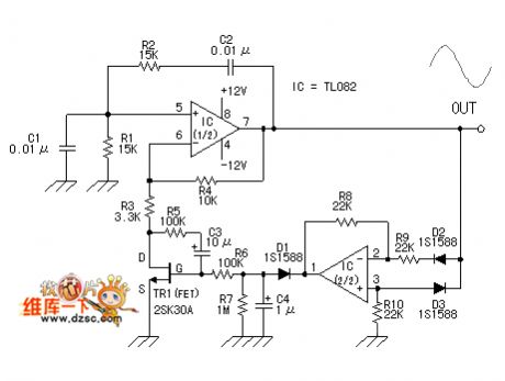
The adjustable voltage-controlled oscillator with large duty cycle
Published:2011/4/18 1:28:00 Author:Ecco | Keyword: adjustable, voltage-controlled oscillator , large duty cycle
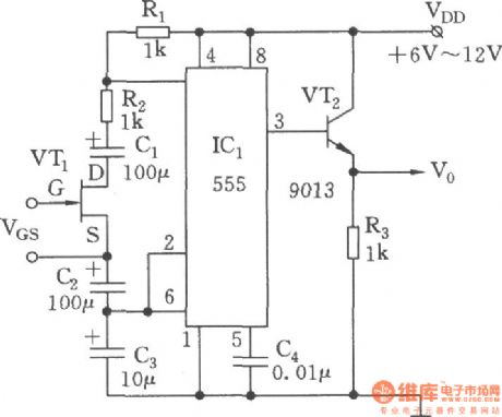
Voltage-controlled oscillator circuit is as shown. 555, R1, R2, C1 ~ C3 and VT1 form a voltage-controlled multivibrator, FET (JFET) VT is voltage-controlled resistor, which can change the impedance between VT-drain (D) and source (S) by changing the gate-source voltage VGs. The coupled capacitors C1、C2 are connected to D,S of VT, they are used to prevent the influence from rest of the circuit of the DC voltage on the JFET. If making coupling capacitors have no effect on the charging and discharging time of time base circuit, the size of C1, C2 should be 10 times of the timing capacitor C3. The advantages of this circuit: the changing of gate-source voltage VGs can make an adjustable variable resistor Rx (can be as large as several hundred kΩ), then it gets the changing of duty cycle and the cycle.
(View)
View full Circuit Diagram | Comments | Reading(2661)
Voltage controlled oscillator with Vc-side controlling duty cycle
Published:2011/4/18 0:54:00 Author:Ecco | Keyword: Voltage controlled oscillator , Vc-side, controlling , duty cycle
View full Circuit Diagram | Comments | Reading(550)
| Pages:51/54 At 204142434445464748495051525354 |
Circuit Categories
power supply circuit
Amplifier Circuit
Basic Circuit
LED and Light Circuit
Sensor Circuit
Signal Processing
Electrical Equipment Circuit
Control Circuit
Remote Control Circuit
A/D-D/A Converter Circuit
Audio Circuit
Measuring and Test Circuit
Communication Circuit
Computer-Related Circuit
555 Circuit
Automotive Circuit
Repairing Circuit