
Oscillator Circuit
Index 44
GATED_1_kHz_OSCILLATOR(NORMALLY_ON)
Published:2009/6/24 21:06:00 Author:May

This gated 1-kHz oscillator offers press-to-turn-off' operation, A, and waveforms at the out-put of pin 3 and across C1, B. (View)
View full Circuit Diagram | Comments | Reading(0)
GATED_1_kHz_OSCILLATOR(NORMALLY_OFF)
Published:2009/6/24 21:05:00 Author:May

This gated 1-kHz oscillator offers press-to-turn-on operation, A, and waveforms at the out-put of pin3 and across C1, B. (View)
View full Circuit Diagram | Comments | Reading(0)
TTL_OSCILLATOR_FOR_1_MHz_10_MHz
Published:2009/6/24 21:01:00 Author:May
View full Circuit Diagram | Comments | Reading(0)
96_MHz_CRYSTAL_OSCILLATOR
Published:2009/6/24 21:00:00 Author:May


Circuit NotesBy usmg a crystal between 27.5 and 33 MHz,the 3rd harmonic will deliver between82.5 and 99 MHz. (View)
View full Circuit Diagram | Comments | Reading(0)
OVERTONE_CRYSTAL_OSCILLATOR
Published:2009/6/24 20:49:00 Author:May

The crystal element in this circuit is con-nected directly between the base and ground.Capacitor C1 is used to improve the feedback due to the internal capacitances of the transis-tor. This capacitor should be mounted as close as possible to the case of the transistor. The LC tank circuit in the collector of the transistor is tuned to the overtone frequency of the crystal.The emitter resistor capacitor must have a capacitive reactance of approximately 90 ohms at the frequency of operation. The tap on induc-tor L1 is used to match the impedance of the collector of the transistor. In most cases, the optimum placement of this tap is approximately one-third from the cold end of the coil. The placement of this tap is a trade-off between stability and maximum power output. The out-put signal is taken from a link coupling coil, L2, and operates by transformer action. (View)
View full Circuit Diagram | Comments | Reading(0)
HIGH_FREQUENCY_CRYSTAL_OSCILLATOR
Published:2009/6/24 20:42:00 Author:May
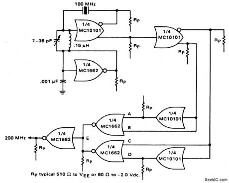
Circuit NotesOne section of the MC10101 is connected as a 100 MHz crystal oscillator with the crystal in series with the feedback loop. The LO tank circuit tunes the 100 MHz harmonic of the crystal and may be used to calibrate the circuit to the exact frequency. A second section of the MC10101 buffers the crystal oscillator and gives complementary 100 MHz signals. Thefrequency doubler consists of two MC10101 gates as phase shifters and two MC1662 NOR gates. For a 50% duty cycle at the output, the delay to the true and complement 100 MHz signals should be 90'. This may be built pre-cisely with 2.5 ns delay lines for the 200 MHz output or approximated by the two MC10101 gates as shown. (View)
View full Circuit Diagram | Comments | Reading(0)
LOW_FREQUENCY_RELAY_OSCILLATOR
Published:2009/6/24 5:42:00 Author:May

Depending on the value of C and the resistance of the relay coil, and the difference in pull-in and drop-out voltage, this circuit will oscillate at a low frequency. R limits in rush current to capacitor C to a level that the relay contacts can handle. Typically, for a 400-Ω relay, R can be 20 to 440 ohms.Flash rate is approximately 1 cycle/second, depending on the relay. (View)
View full Circuit Diagram | Comments | Reading(0)
AF_POWER_OSCILLATOR
Published:2009/6/24 4:15:00 Author:May

An LM386 audio power IC is set up as a feedback oscillator. Any supply from 6 to 12 V can be used. The circuit can drive a loudspeaker. (View)
View full Circuit Diagram | Comments | Reading(0)
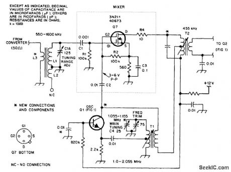
SIMPLE_RF_TEST_OSCILLATOR
Published:2009/6/24 4:13:00 Author:May

A simple oscillator for IF alignment (455 kHz) can prove useful in field testing or where a stan-dard signal generator is available. L1 should res-onate at the desired output frequency with the series combination of C2 and C3. (View)
View full Circuit Diagram | Comments | Reading(1495)
MOSFET_MXER_OSCILLATOR_CIRCUIT_FOR_AM_RECEIVERS
Published:2009/6/24 4:10:00 Author:May
This circuit is an improved front end for upgrading a transistor AM receiver. This front end is useful when the radio is to be used as a tuneable IF amplifier with shortwave converters. (View)
View full Circuit Diagram | Comments | Reading(1948)
COLPITTS_OSCILLATOR
Published:2009/6/24 4:07:00 Author:May
View full Circuit Diagram | Comments | Reading(0)
LC_AUDIO_OSCILLATOR
Published:2009/6/24 4:06:00 Author:May
View full Circuit Diagram | Comments | Reading(0)
NE602_LOCAL_OSCILLATOR_CIRCUITS
Published:2009/6/24 4:05:00 Author:May
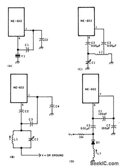
Local oscillator circuits for the NE602. (View)
View full Circuit Diagram | Comments | Reading(0)
26_GHz_OSCILLATOR_FOR_RADAR_SPEED_GUN
Published:2009/6/24 3:19:00 Author:May
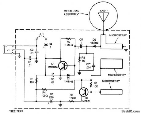
This circuit consists of 2.6-GHz oscillator Q2, a coupling rrticrostripline to ANT1, a 1.1 1/4 wave probe, detector D2, and audio amp Q1. The oscillator feeds power to the antenna, which radiates the signal. The reflected signal from a moving target mixes with the oscillator signal in D2. The resultant beat note (doppler shift) is amplified by Q1 and fed to jack J1, which is used to feed the circuit 12 Vdc. (View)
View full Circuit Diagram | Comments | Reading(2272)
WIEN_BRIDGE_SINE_WAVE_OSCILLATOR_1
Published:2009/6/24 2:56:00 Author:May
View full Circuit Diagram | Comments | Reading(790)
WIEN_BRIDGE_OSCILLATOR_3
Published:2009/6/24 2:55:00 Author:May

View full Circuit Diagram | Comments | Reading(1733)
WIDE_RANGE_OSCILLATOR_FREQUENCY_RANGE_OF_5000_TO_1
Published:2009/6/24 2:54:00 Author:May

Timing resistor R may be adjusted to any value between 10 K and 50 M to obtain a fre-quency range from 400 kHz to 100 Hz. Return-ing the timing resistor to the collector of Q1 ensures that Q1 draws its base current only from the timing capacitor Ct. The timing capacitor recharges when the transistors are off, to a voltage equal to the base emitter volt-age of Q2 plus the base emitter drops ofQ1 and Q2. The transistors then start into conduction. Capacitor Cs is used to speed up the transition. A suitable value would be in the region of 100 pF. (View)
View full Circuit Diagram | Comments | Reading(1001)
TUNABLE_SINGLE_COMPARATOR_OSCILLATOR
Published:2009/6/24 2:53:00 Author:May
Varying the amount of this comparator circuit's hysteresis makes it possible to vary output frequencies in the 740-Hz to 2.7-kHz range smoothly. The amount of hysteresis to-gether with time constant R6C1 determines how much time it takes for C1 to charge or discharge to the new threshold after the output voltage switches. (View)
View full Circuit Diagram | Comments | Reading(1109)
800_Hz_OSCILLATOR
Published:2009/6/24 2:46:00 Author:May

The following transistors may be used: HEP-254, O.C-2, SK-3004, AT30H. To increase the frequency, decrease the value of the capacitors in the ladder network. (View)
View full Circuit Diagram | Comments | Reading(0)
PHASE_SHIFT_OSCILLATOR
Published:2009/6/24 2:45:00 Author:May

A single transistor makes a simple phase shift oscillator. The output is a sine wave with distortion of about 104. The sine wave purity can be increased by putting a variable resistor (25 ohms) in the emitter lead of Q1 (x). The resistor is adjusted so the circuit is only just oscillating, then the sine wave is relatively pure. Operating frequency may be varied by putting a 10 K variable resistor In serles with R3,Or by changing C1,C2,and C3.Making C1,2, 3 equal to 100 nF will halve the operatingfrequency,Operating frequencycanalso bevoltage controlled by a FET In serles with R3,Or optically controlled by an LDR In serles with R3. (View)
View full Circuit Diagram | Comments | Reading(0)
| Pages:44/54 At 204142434445464748495051525354 |
Circuit Categories
power supply circuit
Amplifier Circuit
Basic Circuit
LED and Light Circuit
Sensor Circuit
Signal Processing
Electrical Equipment Circuit
Control Circuit
Remote Control Circuit
A/D-D/A Converter Circuit
Audio Circuit
Measuring and Test Circuit
Communication Circuit
Computer-Related Circuit
555 Circuit
Automotive Circuit
Repairing Circuit