
Oscillator Circuit
Index 45
FEEDBACK_OSCILIATOR
Published:2009/6/24 2:40:00 Author:May

Circuit oscillates because the transistor shifts the phase of the signal 180° from the base to the collector. Each of the RC networks in the circuit is designed to shift the phase 60°at the frequency of oscillation for a total of 180°. The appropriate values of R and C for each network is found from f = 1/2√3πRC); that equation allows for the 60°phase shift required by the design. (View)
View full Circuit Diagram | Comments | Reading(775)
PHASE_SHIFT_OSCILLATOR
Published:2009/6/24 2:33:00 Author:May

ircuit uses a simple RC network to pro-duce an exceptionally shrill tone from a minia-ture speaker. With the parts values shown, the circuit oscillates at a frequency of 3.6 kHz and drives a miniature 2 1/2 speaker with ear-piercing volume. The output waveform is a square wave with a width of 150 pts, sloping rise and fall times, and a peak-to-peak amplitude of 4.2 volts (when powered by 9 volts). Current drain of the oscillator is 90 mA at 9 volts, and total power dissipation at this voltage is 0.81 watt, which is well below the 1.25 watts the 14-pin version will absorb (at room temperature) before shutting down. (View)
View full Circuit Diagram | Comments | Reading(0)
SIMPLE_CODE_PRACTICE_OSCILLATOR
Published:2009/6/24 2:33:00 Author:May

With only a minor circuit change, the basic LM3909 oscillator configuration can be turned into a code-practice oscillator. (View)
View full Circuit Diagram | Comments | Reading(0)
WIEN_BRIDGE_SINE_WAVE_OSCILLATOR
Published:2009/6/24 2:32:00 Author:May

Using the 2N5457 JFET as a voltage vari-able resistor in the amplifier feedback loop, produces a low distortion, constant amplitude sine wave getting the amplifier loop gain just right. The LM103 zener diode provides the voltage reference for the peak sine wave amplitude. (View)
View full Circuit Diagram | Comments | Reading(0)
EASILY_TUNED_SINE_SQUARE_WAVE_OSCILLATORS
Published:2009/6/24 2:31:00 Author:May

This circuit will provide both a sine and square wave output for frequencies from below 20 Hz to above 20 kHz. The frequency of oscillation is easily tuned by varying a single resistor. (View)
View full Circuit Diagram | Comments | Reading(0)
SINE_WAVE_OSCILLATOR
Published:2009/6/24 2:31:00 Author:May

The oscillator delivers a high-purity sinusoid with a stable frequency and amplitude. (View)
View full Circuit Diagram | Comments | Reading(0)
AUDIO_OSCILLATOR
Published:2009/6/24 2:30:00 Author:May

Almost any transistor will work. R1 and C1 will vary the tone. (View)
View full Circuit Diagram | Comments | Reading(0)
WIEN_BRIDGE_OSCILLATOR_2
Published:2009/6/24 2:27:00 Author:May

View full Circuit Diagram | Comments | Reading(618)
WIEN_BRIDGE_OSCILLATOR_1
Published:2009/6/24 2:26:00 Author:May

Wien bridge sine-wave oscillator using two RCA CA3140 op amps covers 30 Hz to 100 kHz with less than 0.5 percent total harmonic distortion. The 10k pot is adjusted for the best waveform. Capacitor C1 and C2 are a two-gang, 450-pF variable with its frame isolated from ground. Maximum output into a 600-ohm load is about 1 volt rms. (View)
View full Circuit Diagram | Comments | Reading(1627)
WIEN_BRIDGE_OSCILLATOR
Published:2009/6/24 2:24:00 Author:May
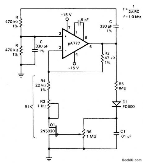
Field effect transistor, Q1, operates in the linear resistive region to provide automatic gain control. Because the attenuation of the RC network is one-third at the zero phase-shift oscillation frequency, the amplifier gain de-termined by resistor R2 and equivalent resis-tor RI must be just equal to three to make up the unity gain positive feedback requirement needed for stable oscillation. Resistors R3 and R4 are set to approximately 1000 ohm less than the required RI resistance. The FET dynami-cally provides the trimming resistance needed to make RI one-half of the resistance of R2. The circuit composed of R5, D1, and C1 iso-lates, rectifies, and filters the output sine wave, converting it into a dc potential to con-trol the gate of the FET. For the low drain-to-source voltages used, the FET provides a symmetrical linear resistance for a given gate-to-source voltage. (View)
View full Circuit Diagram | Comments | Reading(0)
48MHz HCMOS Oscillator
Published:2011/7/29 2:03:00 Author:Ecco | Keyword: 48MHz, HCMOS, Oscillator
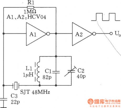
The figure shows the 48MHzcrystal oscillator composed of HCMOS IC. The fundamental frequency of the crystal is l6MHz, butit works in the third harmonic oscillator by force. Harmonic oscillator suppresses the fundamental frequency of the crystal, the parallel resonant circuit in the figure resonances on the base frequenciesof crystal. Connecting to crystal SJT in series may have the highest impedance to fundamental frequency, which can effectively inhibit the fundamental frequency oscillations andensure the third harmonic being easy to start up.
(View)
View full Circuit Diagram | Comments | Reading(1479)
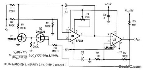
Wideband sine wave VCO composed of LF356N
Published:2011/7/29 2:10:00 Author:Ecco | Keyword: Wideband , sine wave, VCO
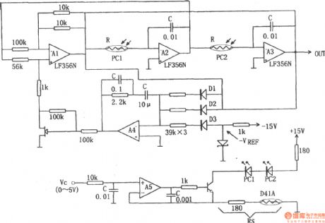
The chart shows the wideband sine wave VCO. Oscillation frequency of the circuit is decided by the resistor R and capacitor C , andthe applied voltage Vc and controlling resistor R constitute theVCO. Variable resistor in the circuit uses photo coupler PC1 and PC2, the rectifier circuit adopts average detection mode. The actual operating frequency of the circuit is tens of Hz or more. In addition, the characteristics of the control voltage Vc with respect to the oscillation frequency depends on the characteristics of optocouplers. The light source of optocoupler is LED and it needs current driving, so the circuit uses the constant current source circuit composed of 4559 operational amplifier. Voltage / current conversion uses Rs, Rs can choose the maximum control voltage Vc freely. In the circuit, IFmax = 30mA, Vcmax = 5V, resistor Rs = 180Ω.
(View)
View full Circuit Diagram | Comments | Reading(2049)
SINUSOIDAL_3_Hz_TO_300_kHz_VCO
Published:2009/6/23 4:15:00 Author:May
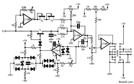


This circuit uses Analog Devices' AD639 universal trigonometric function generator to convert a triangle waveform, the basic waveform of the VCO itself, into a very low-distortion sine wave.By using the AD639 in its frequency tripler mode [2], the frequency range 3 Hz to 300 kHz is now covered. The circuit has been drawn here so that the oscillator loop, consisting of Q1, the integrator and the LT1011 comparator, is clearly shown.When Q1 is off, the input amplifier, which is adjusted to have a gain of exactly -1, pulls a current VIN/R, where R is 5.1 kΩ in series with two JFETs, and Q2 and Q3, out of the virtual earth of the in-tegrator. The output of the integrator thus rises at a rate of VIN/CR, where C = 470 pF. At a level that can be adjusted by the 5-kΩ potentiometer, the comparator flips and turns on Q1.A current of exactly 2VIN/R, is now supplied to the virtual earth of the integrator because there are now two 5.1-kΩ resistors in parallel and only a single JFET in between the virtual earth and Vin.The integrator output now falls at a rate of VIN/CR and the cycle repeats. Any offset in the current to the virtual earth of the integrator, due to circuit board leakage, etc., can be corrected by adjusting the 50-kΩ potentiometer. It follows that the symmetry of the triangle wave at the integrator output can be corrected by adjusting the 2-kΩ potentiometer, and the 50-kΩ potentiometer at VLF, and the frequency can be trimmed with the 5-kΩ potentiometer.The l-kΩ potentiometer variable is adjusted to give the input level to the AD639 needed to drive it over ±270°and so produce a sinusoidal output at three times the frequency of the triangle-wave input. Offset correction for the AD639 is made at the input to the voltage follower by means of the 20-kΩ potentiometer.Once a symmetric triangle wave has been obtained by adjusting the 2-kΩ and 50-kΩ poten-tiometers, and the correct frequency of 100 kHz has been set for VIN/=10 V, by adjusting the 5-kΩ potentiometer, the triple-frequency she-wave output can be set up by adjustment of the 1-kΩ and 20-kΩ potentiometers.This is best done by triggering the CRO from the triangle wave, and then viewing at least three complete cycles of output. Having adjusted for a clean-looking sine wave, the final adjustment of the 1-kΩ and 20-kΩ potentiometers should be made on a single sinusoidal cycle display, using internal trigger so that the three slightly different parts of the output cycle lie one upon the other and can be made to merge. Q1, Q2, and Q3 are 2N4391s, the two Schottlqr diodes are 5082-2810, and the other nine diodes are 1N914.All device power supply pins should be decoupled with 0.33 p.F. Resistors associated with the in-puts of the devices should be 1% high-stability parts. (View)
View full Circuit Diagram | Comments | Reading(3086)
10_Hz_TO_10_kHz_3_DECADE_VCO
Published:2009/6/23 4:37:00 Author:May
View full Circuit Diagram | Comments | Reading(0)
SIMPLE_TLO82_VCO
Published:2009/6/23 4:32:00 Author:May

This circuit uses a dual operational amplifier (TL082) to form a voltage-controlled oscillator (VCO). With the component values shown, the output-frequency range is 100 Hz to 10 kHz when the input control voltage is between 0.05 and 10 V. (View)
View full Circuit Diagram | Comments | Reading(0)
HARTLEY_OSCILLATOR
Published:2009/6/23 2:35:00 Author:May
This circuit uses a tapped inductor in a Hartley oscillator circuit. The tap is generally at 25 to 35% total tums in most instances. (View)
View full Circuit Diagram | Comments | Reading(925)
TUNED_COLLECTOR_OSCILLATOR
Published:2009/6/23 2:34:00 Author:May
View full Circuit Diagram | Comments | Reading(1021)
CLAPP_OSCILLATOR_FOR_100_kHz
Published:2009/6/23 2:32:00 Author:May
This Colpitts oscillator is very stable and usable where good stability is needed, but crystal control is not desirable. It is capable of 1 part in 104 to 105 with good-quality components. (View)
View full Circuit Diagram | Comments | Reading(991)
COLPITTS_OSCILLATOR
Published:2009/6/23 2:31:00 Author:May
In this circuit, the oscillator is free-running. (View)
View full Circuit Diagram | Comments | Reading(0)
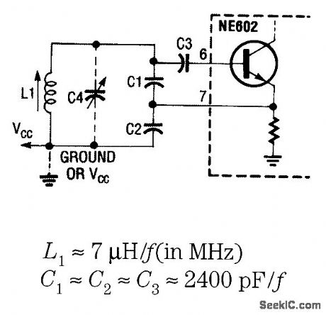
OSCILLATOR_CIRCUITS
Published:2009/6/23 2:31:00 Author:May

These are methods of using an NE602 with a tunable VFO. (View)
View full Circuit Diagram | Comments | Reading(1309)
| Pages:45/54 At 204142434445464748495051525354 |
Circuit Categories
power supply circuit
Amplifier Circuit
Basic Circuit
LED and Light Circuit
Sensor Circuit
Signal Processing
Electrical Equipment Circuit
Control Circuit
Remote Control Circuit
A/D-D/A Converter Circuit
Audio Circuit
Measuring and Test Circuit
Communication Circuit
Computer-Related Circuit
555 Circuit
Automotive Circuit
Repairing Circuit