
Oscillator Circuit
Index 50
FET oscillator circuit
Published:2011/5/19 0:43:00 Author:John | Keyword: FET oscillator

FET oscillator circuit is shown below.
(View)
View full Circuit Diagram | Comments | Reading(1078)
Fre-tech,fretech
Published:2011/5/23 18:49:00 Author:Michel | Keyword: Fre-tech, fretech
Our company,Shanghai Bozhen Electronics Co.,Ltd is the only agent of Fre-tech's(www.fre-tech.com) military and astronautics class crystal oscillatorsin Chinaand our telephone is 021-59773048.
Welcome to reprint theinformation and itis from www.dzsc.com. (View)
View full Circuit Diagram | Comments | Reading(870)
Principle and Circuit of Transformer Feedback Type Oscillator
Published:2011/6/10 7:27:00 Author:Michel | Keyword: Transformer, Feedback Type, Oscillator, Principle and Circuit
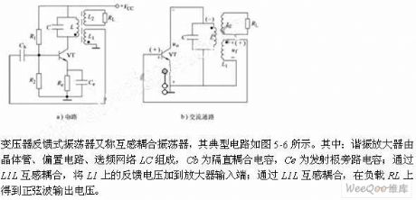
The transformer feedback oscillator is also called mutual-inductance coupling oscillator and it's typical circuit is showed as picture 5-6.The resonant amplifier is composed of transistor,bias circuit and frequency network.Cb is blocking couplingcapacitor,Ce is emittingbypass capacitor .It is coupled via L1L and the L1 feedback voltage is added to amplifier's input end.The sine wave output voltage obtained from load RL by L1L mutual-inductance coupling. (View)
View full Circuit Diagram | Comments | Reading(740)
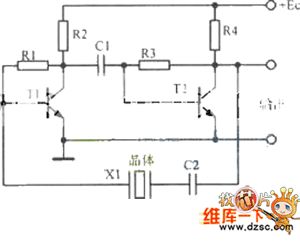
Oscillator Circuit of Three - Point Capacitance
Published:2011/6/10 7:14:00 Author:Michel | Keyword: Three - Point Capacitance, Oscillator Circuit
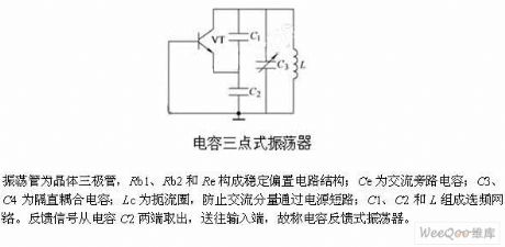
The oscillating tube is rystcal triode and Rb1,Rb2 and Re consititute stable bias circuit.Ce is AC shunt capacitor,itC3 and C4 is blocking coupling capacitor.Lc is choke which prevent the AC componet from passing through the power short-circuit.C1,C2 and L constitute frequency network.The feedback signals output from capcitance C2 and they are transmitted to input end,thus it is called capacitance feedback oscillator. (View)
View full Circuit Diagram | Comments | Reading(963)
Waveform and Low Distortion SLF Two-phase Oscillation Circuit
Published:2011/6/5 8:06:00 Author:Michel | Keyword: Waveform, Low Distortion, SLF, Two-phase Oscillation Circuit
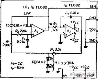
Circuit's Functions
The phase oscillator which can get SIN and COS waves is often used as AC motor signal generator and can also be used as signal source of orthogonal coordinate transformation and adopted as graphic display of X and Y monitor.This circuit is oscillation stability circuit without AGC loop and it can obtain oscillation output when it is low frequency.
Circuit's Work PrincipleOP amplifier,A1 constitutes level 2 low-pass filter,cutoff frequency's phase lags 90 degree, the amplitude is -3DB and integral circuit has nothing to do with the frequency.But it lags 270 degree,the whole circuit produces 360-degree phase shift. (View)
View full Circuit Diagram | Comments | Reading(780)
32768Hz crystal oscillator circuit
Published:2011/6/4 9:35:00 Author:John | Keyword: crystal oscillator
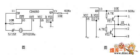
It consists of an integrated circuit CD4060, a crystal with resonant frequency of 30720Hz and other components. CD4060 is a 14-bit binary serial counter, divider and oscillator.
This circuit uses an external 30720Hz crystal to form a crystal oscillator. The oscillation signal is frequency processed through the inner parts of CD4060 and is to output accurate 60Hz frequency signal at the end of Q9 (30720 ÷ 29 = 60Hz). When the circuit is equipped with the double negative digital clock, 2b circuit shown in figure 2 can be used for polarity transform. VT1 and VT2 both use NPN type transistor, such as 9013 and 8050 and so on. Terminal A in the figure is equipped with positive power supply and Terminal B is equipped with negative power supply.
(View)
View full Circuit Diagram | Comments | Reading(2825)
VCO circuit
Published:2011/6/4 10:17:00 Author:John | Keyword: VCO
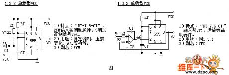
There are many monostable type VCO, which are all rather complex. For simplicity, we just divide it into 2 different units. The circuit without any auxiliary devices is 1.3.1. The circuit using transistors, operational amplifier and other auxiliary devices is 1.3.2. 2 common used circuits are shown in the figure.
1) Features: RT-7.6-CT , the end 2 is input with modulated pulse and the end 5 is set by modulated signal Vct 5.
2) Functions: modulation of pulse width, change of voltage-frequency, A / D change
3) Alias: PWM
(View)
View full Circuit Diagram | Comments | Reading(705)
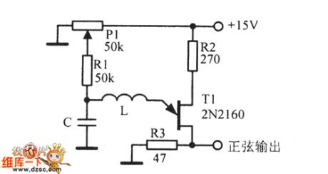
50kHz Sine wave oscillator circuit diagram
Published:2011/6/1 6:41:00 Author:Lucas | Keyword: 50kHz, Sine wave , oscillator
View full Circuit Diagram | Comments | Reading(893)
The light and signal circuit of DPCA-VOLCANE DC7140 ZX
Published:2011/5/19 19:48:00 Author:Borg | Keyword: light and signal circuit, DPCA-VOLCANE
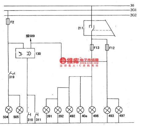
The transmission between high and low beams is fulfilled by pulling the handling behind.
The lighting and signal circuit of DPCA-VOLCANE DC7140 ZX40e-position indicator; 130-alarm for not-off light; 211-left combination switch; 310,311-left-right front door lamp switch; 319-brake lamp switch; 391.392-left and right license lamp; 492,493-left-front and right-front position lamp; 496,497-left-rear and right-rear position lamp; 504,505-left and right brake lamp; 589-danger alarm lamp switch. (View)
View full Circuit Diagram | Comments | Reading(556)
INA217 Signal And Power Supply Basic Connection Circuit
Published:2011/5/17 21:42:00 Author:Robert | Keyword: Signal, Power Supply, Basic Connection
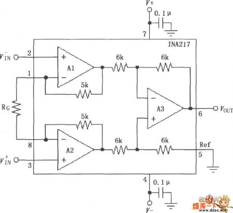
The INA217 Signal And Power Supply Basic Connection Circuit is shown below.
(View)
View full Circuit Diagram | Comments | Reading(730)
Sine oscillating circuit diagram
Published:2011/3/23 20:03:00 Author:may | Keyword: Sine oscillating

The diagram is circuit which consists of VD1, VD2 two variable capacitance diodes, its oscillation frequency is concerned with R1、VD1-R2、VD2, in order to adjust frequency range, the capacitances and resistances of two Bridge road branchs must change the same value of number at the same time. So need to use coaxial connecting two potentiometer or duplex capacitors.
(View)
View full Circuit Diagram | Comments | Reading(593)
Electron coupled oscillator circuit
Published:2011/4/11 2:39:00 Author:may | Keyword: Electron coupled oscillator

This circuit connected directly with collector, thus good for heat dissipation, under a given device parameters, the working frequency is 30MHz , the output coupling high frequency is about 0.8W. The following diagram is electron coupled oscillator circuit.
(View)
View full Circuit Diagram | Comments | Reading(844)
Wien bridge sine wave oscillator circuit composed of LM101A
Published:2011/4/20 6:19:00 Author:Ecco | Keyword: Wien bridge , sine wave , oscillator circuit

The chart shows the Wien bridge sine wave oscillator circuit. The amount of negative feedback circuit is determined by the internal resistance of FET. When the peak value of oscillator output reaches the regulated voltage of regulator diode D1, Q2 turns on, then the grid of Q1 FET becomes negative, Q1's drain - source resistance increases, the negative feedback increases, loop gain decreases. Similarly, when the oscillation amplitude decreases, the loop gain will increase, therefore, it can maintain a certain output range. C1, C2, R1 and R2 constitute a positive feedback loop to ensure the circuit oscillation. Connecting a l00kΩ resistor between drain and gate or gate and source of FET will ensure the FET working in the linear region and reducing distortion. Circuit oscillation frequency: f0 = 1/2π. According to the component value of the figure, the oscillation frequency R1C1 is calculated approximately 1.6kHz. (View)
View full Circuit Diagram | Comments | Reading(2327)
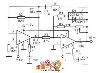
Low power Wien bridge oscillator composed of MC1454
Published:2011/4/21 6:07:00 Author:Ecco | Keyword: Low power , Wien bridge , oscillator


The chart shows the low power Wien bridge oscillator circuit. The circuit is characterized by little distortion when driving low impedance load and large capacitive loads. Operational amplifier used in the circuit could drive 8 ~ 10Ω load, the 10Ω load can provide 2 ~ 4V peak output voltage and the frequency is from 1Hz to 100kHz, distortion is less than 0.5%. Automatic gain control is achieved by a lamp L as the resistance of the bulb changing with the output voltage. Resistor R3 forms a negative feedback loop to determine the output signal amplitude. Capacitors C1 and C2, resistors R1 and R2 constitute a positive feedback. If the value of resistor R1 and the input impedance of the amplifier is equal, R2 = R1 / 2, C1 = C2, then the oscillation frequency; f0 = 1/2π,R1C1C3 is the high-frequency compensation capacitor. The following table lists the relationship between frequency and capacitance C1 (C2) .
(View)
View full Circuit Diagram | Comments | Reading(1183)
COLPITTS Oscillator Circuit Using Crystal
Published:2011/4/26 5:48:00 Author:Robert | Keyword: Crystal, COLPITTS Oscillator

View full Circuit Diagram | Comments | Reading(670)
800Hz oscillator
Published:2011/4/20 5:43:00 Author:Ecco | Keyword: 800Hz , oscillator

The circuit shown in the chart is 800Hz oscillator with the advantages of simple circuit, high accuracy of frequency and stable output level. It consists of four operational amplifiers Manifold Al ~ A3 (LM324) and the 800Hz oscillator composed of SJT (YYZ-2-800Hz) tuning fork. When 800Hz oscillation signal produced by SJ1 being added to two-stage operational amplifier formed by A1 and A2, it will be output by pin ⑦ and become positive feedback frequency signal through the resistor R5, SJT. Then the amplified 800Hz is amplified by A3 again. And it will be sent by pin ⑧ to the potentiometer RP, the adjustable arm can output (Uo) 800Hz sine wave signal. Among them, adjusting the potentiometer RP will meet the output level of 0dB/600Ω, adjustable range is ± 3db. (View)
View full Circuit Diagram | Comments | Reading(1207)
Crystal oscillator and divider(74LS04)
Published:2011/4/20 7:02:00 Author:Ecco | Keyword: Crystal oscillator , divider

View full Circuit Diagram | Comments | Reading(1718)
70MHz parallel crystal oscillator
Published:2011/4/20 22:47:00 Author:Ecco | Keyword: 70MHz, parallel, crystal oscillator

The chart shows 70MHz parallel crystal oscillator circuit. The oscillator is mainlycomposed ofthe transistor VTl, crystal SJT and capacitor Cl, C5 and other components. Selection ofcomponents: capacitors Cl, 20p, C2 to 100p, C3, C7 to 820p, C4 to 56p, C5, C8 to 47p, C6 to 47μF/50V. Inductor Ll is 22μH (color code inductance), L2 is 0.3μH. Resistor Rl is 1.6kΩ, R2 is 1kΩ, R3 is 750Ω, R4 is 180Ω, 1W, R5 is 1.3kΩ, R6 is 3kΩ, R7 is 360Ω, R8 is 470Ω, R9 ~ R12 is 300Ω, 2W. Transistor VTl, VT2choose 3DG828, 65 ≤ β ≤ 115. Crystal SJTchooses JA98-70MHz. Relay KM is JUC-1M.
(View)
View full Circuit Diagram | Comments | Reading(803)
ZXB-2 Type Quartz Crystal Oscillator Circuit
Published:2011/4/23 8:56:00 Author:Robert | Keyword: Quartz Crystal Oscillator
View full Circuit Diagram | Comments | Reading(613)
0.001Hz Sine Wave Oscillator Circuit
Published:2011/4/21 20:25:00 Author:Robert | Keyword: 0.001Hz, Sine Wave, Oscillator
0.001Hz sine wave oscillator circuit is shown below:
(View)
View full Circuit Diagram | Comments | Reading(889)
| Pages:50/54 At 204142434445464748495051525354 |
Circuit Categories
power supply circuit
Amplifier Circuit
Basic Circuit
LED and Light Circuit
Sensor Circuit
Signal Processing
Electrical Equipment Circuit
Control Circuit
Remote Control Circuit
A/D-D/A Converter Circuit
Audio Circuit
Measuring and Test Circuit
Communication Circuit
Computer-Related Circuit
555 Circuit
Automotive Circuit
Repairing Circuit