
Oscillator Circuit
Index 49
TRIANGLE_WAVE_OSCILLATOR
Published:2009/6/17 2:57:00 Author:May

U1-b acts as an integrator while U1-a is a threshold detector. R2 sets the trip level and therefore the amplitude. R3 controls charging current of C1 and the frequency. (View)
View full Circuit Diagram | Comments | Reading(1638)
CODE_PRACTICE_OSCILLATOR
Published:2009/6/17 2:48:00 Author:May

The tone and volume of the sound produced when the telegraph key is depressed can be varied in this code practice oscillator. (View)
View full Circuit Diagram | Comments | Reading(2)
MORSE_PRACTICE_OSCILLATOR
Published:2009/6/17 2:47:00 Author:May

A 555 timer configured as an astable multivibrator is used in this circuit to generate an audio note. C1 can be changed to vary the audio note as desired. (View)
View full Circuit Diagram | Comments | Reading(1124)
QRP_SIDETONE_GENERATOR_CODE_PRACTICE_OSCILLATOR
Published:2009/6/17 2:44:00 Author:May

For use with low-power transmitters with a positive keying voltage. Q1/Q2/Q3 form a switching amplifier. When the key is pressed, the collector of Q3 goes to ground, tuming on Q5 and activating IC1, an audio oscillator. Q4 drives the speaker. For use as a code practice oscillator, insert P1 and J1 and a key in J2. (View)
View full Circuit Diagram | Comments | Reading(940)
LIGHT_CONTROLLED_OSCILLATOR
Published:2009/6/17 2:42:00 Author:May

This circuit can be used as a light detector and possibly as an aid for the visually handi-capped. The frequency of the oscillator is deter-mined by the amount of illumination striking LDR4. (View)
View full Circuit Diagram | Comments | Reading(799)
UNUSUAL_HALL_EFFECT_OSCILLATORS
Published:2009/6/16 22:01:00 Author:May

Although not intended for this application, Hall-effect switch can be used as the basis for a rather unusual oscillator. The oscillator can be reconfigured, as shown in Fig. B, to allow the circuit's oscillating frequency to be controlled via an RC network, comprised of RI and C1. (View)
View full Circuit Diagram | Comments | Reading(1631)
CRYSTAL_CONTROLLED_HARTLEY_OSCILLATOR
Published:2009/6/15 21:23:00 Author:May

View full Circuit Diagram | Comments | Reading(730)
PIERCE_OSCILLATOR
Published:2009/6/15 21:22:00 Author:May
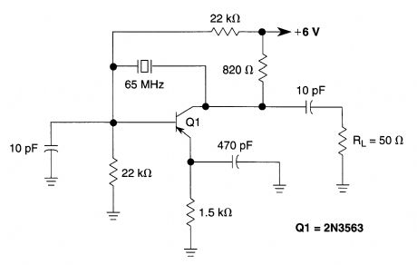
This Pierce oscillator uses a fundamental-mode 65-MHz crystal. (View)
View full Circuit Diagram | Comments | Reading(334)
WIDE_RANGE_CRΥSTAL_OSCILLATOR
Published:2009/6/15 21:21:00 Author:May
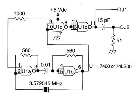
A circuit using one 7400 TTL IC can use crystals of the fundamental type, from 1 to about 13 MHz. Output is rich in harmonics, making this os-cillator useful for calibrations and test applica-tions. (View)
View full Circuit Diagram | Comments | Reading(618)
HEX_BUFFER_CRYSTAL_OSCILLATOR
Published:2009/6/15 21:09:00 Author:May

A 4049 single section acts as a crystal oscilla-tor, driving another section as a buffer, leaving four sections for other use. Use a 32- or 20-pF parallel resonant fundamental crystal. (View)
View full Circuit Diagram | Comments | Reading(753)
CRYSTAL_OSCILLATOR
Published:2009/6/15 21:04:00 Author:May
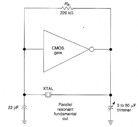
The CMOS amplifier is biased into the linear region by resistor RB. The pi-type crystal network (C1 and C2, and XTAL) provides the 180' phase shift at the resonant frequency which causes the circuit to oscillate. (View)
View full Circuit Diagram | Comments | Reading(1)
Low frequency oscillator (flashing shine circuit) circuit 1 made by 555 time-base circuit
Published:2011/5/12 2:03:00 Author:Ecco | Keyword: Low frequency, oscillator, flashing, shine , 555, time-base circuit

The chart shows a flashing shine circuit, and when the circuit works, twolight-emitting diodes will shine simultaneously. The working principle of the circuit is similar to 555 audio oscillator, the difference is that the capacity of capacitor Clis increased to 4.7μF. Therefore, the circuit's oscillation frequency is very low, the changing rate of potential on pin 3 of NE555 is low. When the output of pin 3is inhigh level, the light-emitting diode VDl, VD2 are lit at the same time. When the output of pin 3is inlow level, the light-emitting diode VDl, VD2 turns off.In the circuit, when the resistance of R3 is higher, the brightnessis smaller; or resistance of R3 is lower, the brightnessis greater. Note:theresistance of R3 should not be too small, otherwise the current flowing through the light-emitting diodes is too high, the power consumption is higher,it will have negative impact on thelight-emitting diode, or even it is burned. Typically, the current flowing through the LED can be controlled between 10 ~ 20mA.
(View)
View full Circuit Diagram | Comments | Reading(1074)
Low frequency oscillator (flashing shine circuit) circuit 2 made by 555 time-base circuit
Published:2011/5/12 2:01:00 Author:Ecco | Keyword: Low frequency , oscillator, flashing, shine , 555 , time-base circuit

The chart shows the flashing shine circuit based on 555 circuit,and when the circuit works, two light-emitting diodes will shine
alternately. The working principle: The NE555 time-base circuit and Rl、R2、Cl form a low frequency oscillator. When the circuit starts oscillation, the level of pin 3 in theNE555 time-base circuitis variable. When pin 3 is in high level, VD1 loses power and doesn't emit light, VD2 gets power and emits light; when pin 3 is inlow level, VD2 loses power and doesn't emit light, VD1 gets power and emit light. So two light-emitting diodes will shine alternately. When doing the circuit, the diodes could choose red, green or yellow, the difference will be more marked.
(View)
View full Circuit Diagram | Comments | Reading(632)
Long cycle on / off multivibrator
Published:2011/5/17 4:02:00 Author:Ecco | Keyword: Long cycle , on , / off , multivibrator

The multivibrator composed of 555 timer IC can adjust the frequency and duty cycle independently, but if the on / off cycle is very long, it needs a large capacity capacitor. The circuit shown as the chart can adjust the on / off cycle flexibly without using large capacitors, and the longest period can reach several hours. It uses CD4020 14-stage binary counter to count the output frequency, the two output terminals Ql4 of CD4020 will rise and fall to connect to the edges Rl and R2, it can output separate off-cycle and on-cycle. The output end Q1 can be used to indicate the continuous cycle. If R2 = 100k time, Ton ≈ 5 minutes; if Rl = 1M time, Toff ≈ 50 minutes.
(View)
View full Circuit Diagram | Comments | Reading(2471)
Quartz Crystal Oscillation Circuit of C-MOS Converter
Published:2011/6/14 13:07:00 Author:Michel | Keyword: C-MOS Converter, Quartz Crystal, Oscillation Circuit
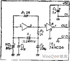
Circuit's Functions Recently,there is a trend that people changes C-MOS for TTL devices.What's more,74HC-series products also got further enrichment.The oscillating circuit composed of C-MOS IC can substitute for clock oscillating circuit composed of level two TTL because TTL IC stops oscillating and causes abnormity easily.However,this circuit is simple with accurate oscillation.
Circuit's Work PrincipleThe partial resistor R1 is connected between input and output ends and make the input end fix on threshold voltage to keep C-MOS changeover job in online linear status. (View)
View full Circuit Diagram | Comments | Reading(609)
Low Distortion and State Variable Two-phase Oscillation Circuit
Published:2011/6/14 13:15:00 Author:Michel | Keyword: Low Distortion, State Variable, Two-phase Oscillation Circuit

Circuit's Functions
The amplifier used in audio equipments needs low distortion signal when it tests.Recently,there are many low distortion OP amplifiers used in audio equipments.If oscillator has distortion, the measurement will be restricted.The state variable circuit has some parts of the active power filter and it can change into oscillators if positive feedback is added.The integrator is composed of two-stage opposite phase amplifier and the high frequency distortion caused by integrator itself reduces 6DB/OCT per stage.This circuit is adopted in low distortion oscillating circuit and if the difference valuefor input and output phase of integrator is 90 degree,it will get 2 phase oscillation output. (View)
View full Circuit Diagram | Comments | Reading(1915)
Ungoverned Quartz Crystal Oscillating Circuit without Inductance L
Published:2011/6/14 21:20:00 Author:Michel | Keyword: Ungoverned Quartz Crystal, Oscillating Circuit
Circuit's Functions
If the transistor's collector load adopts LC resonance loop and the oscillation frequency of Pierce C - B or Boer, B - E circuit must attuned a little deflective to make the oscillation stable.This oscillating circuit can be used if there is no inductance L.
Circuit's Work Principle
If quartz resonator is used as inductance L,it can be used as deformation carat diop oscillating circuit.Capacitor C2 and C3 feedback posistively and the frequency is low and electric capacity is large.
The oscillation frequency reaches 5~20MHZ when capacity is 100PF and a proper capacity can be chosen according to requirements. (View)
View full Circuit Diagram | Comments | Reading(611)
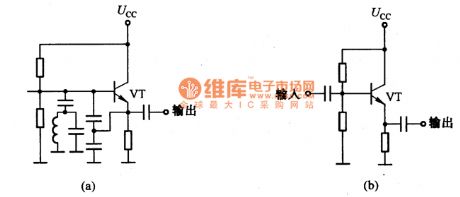
Oscillation circuit of the emitter follower
Published:2011/6/30 13:01:00 Author:Sophia | Keyword: Emitter follower, Oscillation
(View)
View full Circuit Diagram | Comments | Reading(1065)
oscillator composed of gate circuit circuit
Published:2011/6/26 8:36:00 Author:Fiona | Keyword: composed of gate circuit
View full Circuit Diagram | Comments | Reading(553)
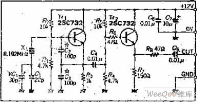
Parallel type crystal oscillator circuit
Published:2011/6/26 9:01:00 Author:Fiona | Keyword: Parallel type, crystal
Among this circcuit, the resistors R1,2 and resistors R5, R6, R7 are the DC bias component of the transistors VT1 and VT2.High-frequency choke coil L2 offers the DC path to the the collector current of the oscillation tube VT1. C2 is the blocking capacitors.C3, C7 are the exchange bypass capacitor which make the emitter of the VTl in exchange zero potential,but the DC-bit is not zero.The inductor L1, capacitor c6,resistor R 3 improve the power supply filter circuit,whose role is to reduce ripple voltage to increase the DC component. Slightly adjustable capacitors can change the size of the coupling signal.
(View)
View full Circuit Diagram | Comments | Reading(573)
| Pages:49/54 At 204142434445464748495051525354 |
Circuit Categories
power supply circuit
Amplifier Circuit
Basic Circuit
LED and Light Circuit
Sensor Circuit
Signal Processing
Electrical Equipment Circuit
Control Circuit
Remote Control Circuit
A/D-D/A Converter Circuit
Audio Circuit
Measuring and Test Circuit
Communication Circuit
Computer-Related Circuit
555 Circuit
Automotive Circuit
Repairing Circuit