Want to post a buying lead? If you are not a member yet, please select the specific/related part number first and then fill the quantity and your contact details in the "Request for Quotation Form" on the left, and then click "Send RFQ".Your buying lead can then be posted, and the reliable suppliers will quote via our online message system or other channels soon.
(•) Pulse width limited by safe operating area (*) Limite d by package
STN1N20 Features
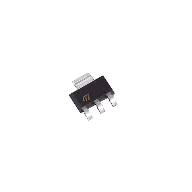
TYPICAL RDS(on) = 1.2 AVALANCHERUGGED TECHNOLOGY SOT-223CAN BE WAVE OR REFLOW SOLDERED AVAILABLEIN TAPEAND REEL ON REQUEST 150 OPERATINGTEMPERATURE APPLICATIONORIENTED CHARACTERIZATION
STN1N20 Typical Application
HARD DISK DRIVERS SMALLMOTOR CURRENT SENSE CIRCUITS DC-DC CONVERTERS AND POWER SUPPLIES
STN1NB80 General Description
Using the latest high voltage MESH OVERLAYTM process, STMicroelectronics has designed an advanced family of power MOSFETs with outstanding performances. The new patent pending strip layout coupled with the Company's proprietary edge termination structure, gives the lowest RDS(on) per area, exceptional avalanche and dv/dt capabilities and unrivalled gate charge and switching characteristics.
STN1NB80 Maximum Ratings
Symbol
Parameter
Value
Unit
VDS
Drain-source Voltage (VGS = 0)
800
V
VDGR
Drain-gate Voltage (RGS = 20 k )
800
V
VGS
Gate- source Voltage
± 30
V
ID
Drain Current (continuos) at TC = 25
0.2
A
ID
Drain Current (continuos) at TC = 100
0.12
A
IDM()
Drain Current (pulsed)
0.8
A
PTOT
Total Dissipation at TC = 25
2.9
W
Derating Factor
0.02
W/
dv/dt (1)
Peak Diode Recovery voltage slope
4
V/ns
Tstg
Storage Temperature
65 to 150
Tj
Max. Operating Junction Temperature
150
(`) Pulse width limited by safe operating area (1) ISD 12 A, di/dt 200 A/s, VDD V(BR)DSS, Tj TJMAX
STN1NB80 Features
TYPICAL RDS(on) = 16 EXTREMELY HIGH dv/dt CAPABILITY 100% AVALANCHE TESTED VERY LOW INTRINSIC CAPACITANCES GATE CHARGE MINIMIZED
STN1NB80 Typical Application
SWITCH MODE POWER SUPPLIES(SMPS) AC ADAPTORS AND BATTERY CHARGERS FOR HANDHELD EQUIPMENT