NDH8501N, NDH8502P, NDH8520C Selling Leads, Datasheet
MFG:NS Package Cooled:SOP8 D/C:09+

NDH8501N, NDH8502P, NDH8520C Datasheet download

Part Number: NDH8501N
MFG: NS
Package Cooled: SOP8
D/C: 09+


MFG:NS Package Cooled:SOP8 D/C:09+

NDH8501N, NDH8502P, NDH8520C Datasheet download

MFG: NS
Package Cooled: SOP8
D/C: 09+
Want to post a buying lead? If you are not a member yet, please select the specific/related part number first and then fill the quantity and your contact details in the "Request for Quotation Form" on the left, and then click "Send RFQ".Your buying lead can then be posted, and the reliable suppliers will quote via our online message system or other channels soon.
TOP
PDF/DataSheet Download
Datasheet: NDH8301N
File Size: 216852 KB
Manufacturer: FAIRCHILD [Fairchild Semiconductor]
Download : Click here to Download
PDF/DataSheet Download
Datasheet: NDH8502P
File Size: 74107 KB
Manufacturer: FAIRCHILD [Fairchild Semiconductor]
Download : Click here to Download
PDF/DataSheet Download
Datasheet: NDH8520C
File Size: 234316 KB
Manufacturer: FAIRCHILD [Fairchild Semiconductor]
Download : Click here to Download
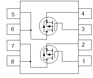
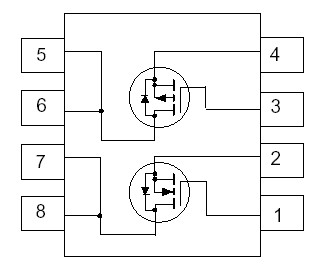
SuperSOTTM-8 P-Channel enhancement mode power field effect transistors are produced using Fairchild's proprietary, high cell density, DMOS technology. This very high density process is especially tailored to minimize on-state resistance. These devices are particularly suited for low voltage applications such as notebook computer power management and other battery powered circuits where fast high-side switching, and low in-line power loss are needed in a very small outline surface mount package.
|
Symbol |
Parameter |
NDH8502P |
Units | |
|
VDSS VGSS |
Drain-Source Voltage Gate-Source Voltage - Continuous |
-30 ±20 -2.2 -10 0.8 -55 to 150 |
V V A W °C | |
|
ID |
Drain Current Continuous Pulsed | (Note 1) | ||
|
PD |
Maximum Power Dissipation | (Note 1 ) | ||
| TJ,TSTG | Operating and Storage Temperature Range | |||
| RJA RJC |
Thermal Resistance, Junction-to-Ambient Thermal Resistance, Junction-to-Case |
(Note 1) (Note 1) |
156 |
°C/W °C/W |

These dual N- and P-Channel enhancement mode power field effect transistors are produced using Fairchild's proprietary, high cell density, DMOS technology. This very high density process is especially tailored to minimize on-state resistance and provide superior switching performance. These devices are particularly suited for low voltage applications such as notebook computer power management and other battery powered circuits where fast switching, low in-line power loss, and resistance to transients are needed.
|
Symbol |
Parameter |
N-Channel |
P-Channel |
Units | |
|
VDSS VGSS |
Drain-Source Voltage Gate-Source Voltage - Continuous |
30 ±20 2.8 10 |
-30 ±20 -2.2 -10 |
V V A W °C | |
|
ID |
Drain Current Continuous Pulsed | (Note 1) | |||
|
PD |
Power Dissipation for Single Operation | (Note 1) |
0.8 -55 to 150 | ||
| TJ,TSTG | Operating and Storage Junction Temperature Range | ||||
| RJA RJC |
Thermal Resistance, Junction-to-Ambient Thermal Resistance, Junction-to-Case |
(Note 1) (Note 1) |
156 |
°C/W °C/W |

