
Circuit Diagram
Index 258
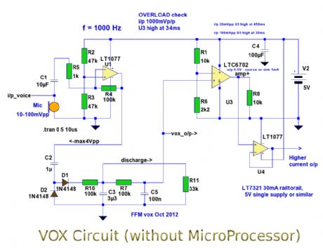
Voice Operated Switch
Published:2012/12/3 0:19:00 Author:muriel | Keyword: Voice Operated Switch
View full Circuit Diagram | Comments | Reading(1530)
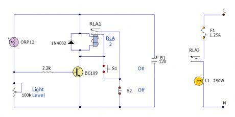
Parking Light Switch
Published:2012/12/3 0:18:00 Author:muriel | Keyword: Parking Light Switch
View full Circuit Diagram | Comments | Reading(722)
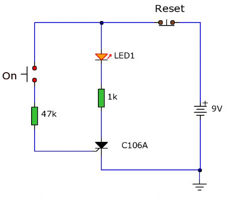
Latch Switch 2
Published:2012/12/3 0:17:00 Author:muriel | Keyword: Latch Switch
View full Circuit Diagram | Comments | Reading(774)
10 Way Electronic Switch
Published:2012/12/3 0:16:00 Author:muriel | Keyword: 10 Way, Electronic Switch
View full Circuit Diagram | Comments | Reading(893)
Toggle Switch No. 3
Published:2012/12/3 0:15:00 Author:muriel | Keyword: Toggle Switch

This versatile circuit provides a selection of different switching modes. It can be used as two entirely separate toggle switches - with each push button successively energizing and de-energizing its own relay. Or the two switches can be interlinked with diodes - to produce a number of different switching patterns. For example - the circuit can be used to reverse the direction of DC motors. (View)
View full Circuit Diagram | Comments | Reading(844)
Keypad Combination Lock
Published:2012/12/3 0:14:00 Author:muriel | Keyword: Keypad Combination Lock

View full Circuit Diagram | Comments | Reading(975)
AC Switch
Published:2012/12/3 0:14:00 Author:muriel | Keyword: AC Switch

View full Circuit Diagram | Comments | Reading(713)
Latch Switch
Published:2012/12/3 0:13:00 Author:muriel | Keyword: Latch Switch

View full Circuit Diagram | Comments | Reading(845)
Toggle Switch No. 2
Published:2012/12/3 0:13:00 Author:muriel | Keyword: Toggle Switch


Pushing the button once will energize the relay. Pushing the same button a second time will de-energize the relay. Any simple momentary action push-to-make switch will do. (View)
View full Circuit Diagram | Comments | Reading(839)
A Thermostat With Adjustable Hysteresis
Published:2012/12/3 0:11:00 Author:muriel | Keyword: Thermostat, Adjustable Hysteresis

A thermostat doesn't try to maintain a constant temperature. In order to do so - it would have to keep switching on and off every few seconds. Instead - it keeps the temperature within a specific range. When the preset temperature has been reached - it switches off. And it only switches on again - when there has been a significant change in temperature.
The difference between the temperature at which the thermostat switches off - and the temperature at which it switches on again - is the hysteresis. Without this hysteresis - your central heating, refrigerator etc. would keep switching on and off every few seconds.
This particular circuit energizes the relay when the temperature falls - and de-energizes the relay when the temperature rises again. If you replace the pnp transistor (BC557) with an npn transistor (BC547) - the circuit will operate the other way round.
In order to minimize power consumption - choose the configuration that energizes the relay for the shorter time period. If it's going to be hot most of the time - choose the one that energizes the relay when the temperature falls (BC557). If it's going to be cold most of the time - choose the one that energizes the relay when the temperature rises (BC547).
(View)
View full Circuit Diagram | Comments | Reading(1867)
The amplifier tube protector circuit
Published:2012/12/2 21:55:00 Author:Ecco | Keyword: Amplifier tube , protector

In the Figure, K is a power switch, T1 is the controlling small power transformer, T2 is the amplifier power transformer. IC1 (S1-S4) is the four - way analog switch CD4066. When the machine is open, K1 is closed, C1 gets 12V DC voltage. The S3 gets conduction because control terminal is high, then S4 control terminal is pulled low, S4 disconnects. C2 voltage can not get mutation, so S1 gets conduction when machines is open due to the control terminal is in high level, and optocoupler IC2 LED is lit.
(View)
View full Circuit Diagram | Comments | Reading(1665)
Flashing light control circuit
Published:2012/12/2 21:37:00 Author:Ecco | Keyword: Flashing light , control

This wonderful scene can be realized through the flashing light control circuit installed below the front headlights or trunk parts. Actual line is shown as the figure. The circuit uses three integrated circuits which are coupled with clever circuit connection, when the motorcycle is driven at night, it can make lanterns flicker constantly to produce aesthetic effect like line flowing water. This flashing light control circuit can also be used for the festive lighting control or other applications. 555 time base circuit is connected to resistors R1, R2 and capacitor C1 to constitute astable multivibrator, and it generates about 5Hz clock signal for counting pulses as decimal / distributor CD4017.
(View)
View full Circuit Diagram | Comments | Reading(1323)
Level test circuit using voltage comparator LM324
Published:2012/12/2 21:54:00 Author:Ecco | Keyword: Level test , voltage comparator
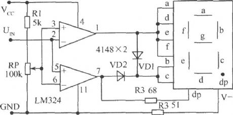
It is facilitate to test the threshold level adjustment, and the DTL, TTL, CMOS, and other logic level. It is known from voltage compator: when the voltage on non -inverting input terminal (positive side) is higher than inverting input terminal (negative side), the comparator output is high; in contrary, the output is low. RP is the comparison voltage adjustment potentiometer, when UIN is higher than the set voltage, the output of pin 7 is high, it displays 1 and the decimal point dp emit light.
(View)
View full Circuit Diagram | Comments | Reading(7232)
High sensitivity anti-theft alarm circuit with high loudness
Published:2012/12/2 21:28:00 Author:Ecco | Keyword: High sensitivity, anti-theft alarm, high loudness
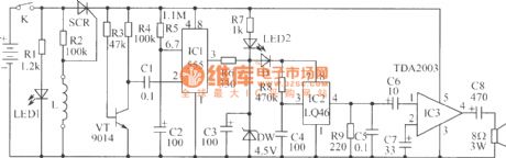
The SCR, R2 and L form a triggered power switch with controllable disconnection, L is an anti-theft wire. Transistor VT and IC1 form approximately 2min monostable delay trigger circuit. IC2 is the language alarm circuit which can emit the sound of catch thief, please . Usually when K is closed, if there is no thief, the alarm burglar lines will make SCR control gate trigger current be short, SCR is off, the circuit does not work, and it is in the probation status. If thied jumps over the wall of park, the wire L is pulled and disconnected, SCR control pole gets triggered current by R2, then it is be turned on to provide the power for working circuit.
(View)
View full Circuit Diagram | Comments | Reading(1149)
The bistable circuit with optocoupler and transistor
Published:2012/12/2 20:37:00 Author:Ecco | Keyword: bistable , optocoupler , transistor
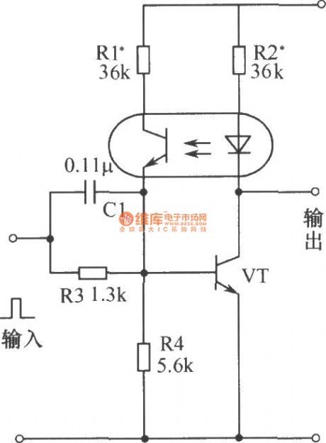
In the initial state with the power turning on, the transistor VT is cutoff, the circuit outputs high potential. When the input terminal is coupled with a positive pulse, the collector current of VT increases, photocoupler light emitting diode emits light, and the collector-emitter resistance of phototransistor becomes smaller, then the base current of VT increases to form a positive feedback, so that VT quickly be saturated, and it changes to 0 from 1 . When it is input the negative pulse, the collector current of VT becomes small, thereby enabling light emitting diode darken, and VT's base current becomes small, causing the collector current of VT to be further reduced, the VT quickly become the OFF state, the light emitting diode does not emit light, the phototransistor is turned off, so that VT is stable in the off state, the state of flip-flop changes from 0 to l .
(View)
View full Circuit Diagram | Comments | Reading(1215)
Pincushion correction circuit 1
Published:2012/11/29 21:08:00 Author:Ecco | Keyword: Pincushion correction
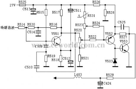
Field sawtooth wave signal is sent into V551's base by R514, then it is integrated by R516 and C514, and E-B differential integrated by C510, R519, C509 and V551 to form parabolic wave signal, then it is amplified by V552 and output from collector, and it is directly sent to V553's base, parabolic wave signal output from V553 collector is added to V402's negative end by R529 and L403 to modulate the current on coil by V401, then the distortion can be corrected.
(View)
View full Circuit Diagram | Comments | Reading(941)
Pincushion correction circuit 3
Published:2012/11/29 21:13:00 Author:Ecco | Keyword: Pincushion correction
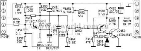
The models using pincushion correction: Korea Samsung MC-15 movement, Venus C6418, V6458, LOWA CT6388W, Peony 64C1. VR451 is the amplitude adjustment potentiometer, VR452 is the Pincushion adjustment potentiometer. Sawtooth voltage is sent to the pincushion correction circuit by P404's pin 4, R455, C454 and R457 form an integrator which integrates sawtooth wave to form a convex parabolic wave voltage.
(View)
View full Circuit Diagram | Comments | Reading(700)
The audio amplifier circuit
Published:2012/11/29 21:19:00 Author:Ecco | Keyword: audio amplifier

When the input signal level is less than 20mW , LM378 op amp directly uses 5Ω resistor to provide up to approximately 100mA peak current for load. When it is greater than 20mW, the load current bias flowing through 5Ω resistor to boost transistor and make it get conduction and increase the output power. Transistor and operational amplifier must be connected to a suitable heat sink.
(View)
View full Circuit Diagram | Comments | Reading(1363)
The coupling circuit with optical fiber transmission data
Published:2012/11/29 21:25:00 Author:Ecco | Keyword: coupling circuit , optical fiber , transmission data
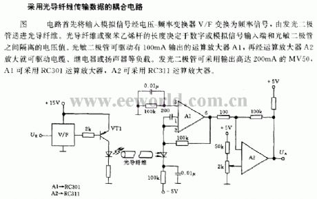
The circuit shown in figure can convert input analog signal into frequency signal by voltage V / F - the frequency converter, then it is sent to the optical fiber by light emitting diode. The length of optical fiber or polystyrene is determined the isolated voltage between the digital or analog signal input terminal and a photodiode. The photodiode can drive operational amplifier A1 with 100mA output.
(View)
View full Circuit Diagram | Comments | Reading(986)
The phonographs amplifier circuit
Published:2012/11/29 21:30:00 Author:Ecco | Keyword: phonographs amplifier

LM387 is one model of LM38X series. LM38X series of products are advanced linear amplifier ICs with low noise, low distortion, wide bandwidth and suppressing fluctuations advantages. In addition, they use a single power supply, internal compensation, power supply decoupling and regulation, larger output voltage changes and larger power bandwidth. 600Ω resistor connected to the pickup head in parallel is used to prevent the current.
(View)
View full Circuit Diagram | Comments | Reading(1144)
| Pages:258/2234 At 20241242243244245246247248249250251252253254255256257258259260Under 20 |
Circuit Categories
power supply circuit
Amplifier Circuit
Basic Circuit
LED and Light Circuit
Sensor Circuit
Signal Processing
Electrical Equipment Circuit
Control Circuit
Remote Control Circuit
A/D-D/A Converter Circuit
Audio Circuit
Measuring and Test Circuit
Communication Circuit
Computer-Related Circuit
555 Circuit
Automotive Circuit
Repairing Circuit