
Circuit Diagram
Index 243
Digital circuit sound and light control stairs delay switch circuit ( 1 )
Published:2012/12/13 0:43:00 Author:Ecco | Keyword: Digital circuit, sound and light, control , stairs delay switch
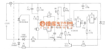
It has all the characteristics of the discrete components circuit, it also has high delay accuracy, high operational reliability and low the discrete nature performance between the various finished products, and therefore very suitable for factory mass production. The circuit has two characteristics: Firstly, the lamp operating time is the soft-start and half-wave AC after being lit, which can greatly extend the service life of the lamp; secondly, lamp lighting time is determined by the time constant of R10 and C5.
(View)
View full Circuit Diagram | Comments | Reading(1304)
Voltage positive pulse peak holding circuit diagram
Published:2012/12/13 0:51:00 Author:Ecco | Keyword: Voltage, positive pulse, peak holding

Voltage positive pulse peak holding circuit diagram is shown as below:
(View)
View full Circuit Diagram | Comments | Reading(1253)
The internal structure schematic diagram of UC3907 IC chip
Published:2012/12/13 1:00:00 Author:Ecco | Keyword: internal structure , IC chip
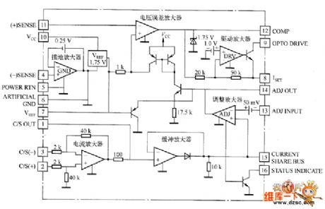
Operating supply voltage range V (10 feet) is 4.5 ~ 35 V; chip has a reference voltage source VREF, and its value relative to ARTIFICIAL GND (6 feet ) is 1.15 V which can output from VREF (7 feet ); ARTIFICIAL GND is the low resistance ground ( ground reference ) of chip, and its level is higher 0.25V than (-) SENSE (4 feet), and the voltage bias provides loop circuit for the the grounded amplifier current, while the voltage sampling negative terminal ( - ) Sense ( i.e. grounded amplifier inverting input terminal ) has a high input impedance.
(View)
View full Circuit Diagram | Comments | Reading(1422)
The FM optical receiver circuit diagram
Published:2012/12/13 0:49:00 Author:Ecco | Keyword: FM , optical receiver
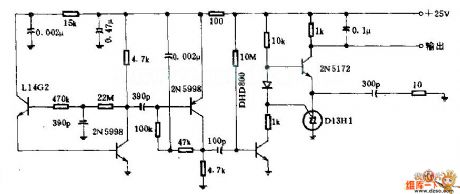
This circuit is applied to the pulse rate modulation system. In this system, the transmitter changes the pulse rate of modulated light speed in optical fiber, so that the vertical variation is around the frequency of 50kHz center. L14G2 phototransistor converts modulated light to RF signal to restore the original audio signal.
(View)
View full Circuit Diagram | Comments | Reading(1093)
PVDF heart sound pulse measurement principle circuit
Published:2012/12/13 1:17:00 Author:Ecco | Keyword: PVDF , heart sound , pulse measurement
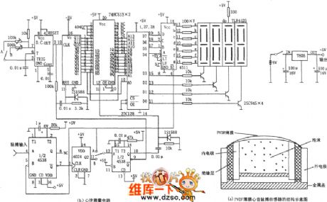
Measuring circuit is composed of monostable oscillator ( 4538 ), the divider ( 4024), pulse generator ( ICM7555 ), counter ( 4040), latch ( 74HC513 ), memory ( ROM ), seven-segment latch drive ( 7511 ) and seven-segment digital LED tube. Figure (a) is a structural diagram of the PVDF heart sound pulse sensor. In Figure ( a ), PVDF film is dome-shaped and slightly protruding outward to make a good contact with the skin surface. The PVDF material is flexible to close to the skin, the impedance is matching with the skin, subsequently, even under stress, the pressure does not affect the detection pulse pressure variation, and therefore able to detect a slight ripple signal.
(View)
View full Circuit Diagram | Comments | Reading(2085)
3 volt LED chaser
Published:2012/12/12 21:22:00 Author:muriel | Keyword: 3 volt, LED chaser
View full Circuit Diagram | Comments | Reading(2649)
LED Chasers
Published:2012/12/12 21:22:00 Author:muriel | Keyword: LED Chasers

View full Circuit Diagram | Comments | Reading(1070)
cascode BJT RF amplifier 2
Published:2012/12/12 21:21:00 Author:muriel | Keyword: cascode , BJT , RF amplifier

View full Circuit Diagram | Comments | Reading(2698)
Experimentation With Variable Q1 Emitter Degeneration
Published:2012/12/12 21:19:00 Author:muriel | Keyword: Variable Q1, Emitter Degeneration

View full Circuit Diagram | Comments | Reading(703)
fixed Q1 and Q2 bias version
Published:2012/12/12 21:19:00 Author:muriel | Keyword: Q1, Q2, bias version

View full Circuit Diagram | Comments | Reading(692)
fixed bias version
Published:2012/12/12 21:18:00 Author:muriel | Keyword: fixed bias version

View full Circuit Diagram | Comments | Reading(633)
cascode 2N3904 IF amplifier
Published:2012/12/12 21:17:00 Author:muriel | Keyword: cascode , 2N3904, IF amplifier

View full Circuit Diagram | Comments | Reading(4311)
cascode amplifier
Published:2012/12/12 21:17:00 Author:muriel | Keyword: cascode amplifier

View full Circuit Diagram | Comments | Reading(0)
Understanding Voltage Divider
Published:2012/12/12 21:16:00 Author:muriel | Keyword: Understanding Voltage Divider

View full Circuit Diagram | Comments | Reading(739)
Cascode BJT RF Amplifier
Published:2012/12/12 21:14:00 Author:muriel | Keyword: Cascode, BJT, RF Amplifier

View full Circuit Diagram | Comments | Reading(2631)
5 MHz WWV Cascode Bipolar Amplifier
Published:2012/12/12 21:13:00 Author:muriel | Keyword: 5 MHz , WWV Cascode, Bipolar Amplifier

View full Circuit Diagram | Comments | Reading(953)
40-41 meter band active antenna
Published:2012/12/12 21:12:00 Author:muriel | Keyword: 40-41 meter , band active antenna

View full Circuit Diagram | Comments | Reading(815)
Tuning a Whip To Other Frequencies
Published:2012/12/12 21:11:00 Author:muriel | Keyword: Tuning, Whip, Other Frequencies

View full Circuit Diagram | Comments | Reading(642)
broadband version W7ZOI
Published:2012/12/12 21:10:00 Author:muriel | Keyword: broadband version, W7ZOI

The broadband version W7ZOI suggested to try building. I modified the output transformer in the Figure 6 project and tested it with Tom, VE7TW. We really liked it. By adjusting the network trimmer capacitor, I was also able to tune the 30 meter Amateur radio band as well. For 30 meter band use, I peaked the tank circuit at 10.125 MHz by listening to receiver noise with a home brew direct conversion receiver and was suitably impressed.
This is the active antenna design I wll use for my future projects where strong voltage gain is required. If your receiver has a higher impedance such as 500 ohms, you might try using a couple more links on the output transformer secondary winding.
(View)
View full Circuit Diagram | Comments | Reading(2860)
Cascode JFET Amplifier Version
Published:2012/12/12 21:09:00 Author:muriel | Keyword: Cascode JFET Amplifier

View full Circuit Diagram | Comments | Reading(1316)
| Pages:243/2234 At 20241242243244245246247248249250251252253254255256257258259260Under 20 |
Circuit Categories
power supply circuit
Amplifier Circuit
Basic Circuit
LED and Light Circuit
Sensor Circuit
Signal Processing
Electrical Equipment Circuit
Control Circuit
Remote Control Circuit
A/D-D/A Converter Circuit
Audio Circuit
Measuring and Test Circuit
Communication Circuit
Computer-Related Circuit
555 Circuit
Automotive Circuit
Repairing Circuit