
Circuit Diagram
Index 244
Common Gate Amplifier Version
Published:2012/12/12 21:09:00 Author:muriel | Keyword: Common Gate Amplifier

View full Circuit Diagram | Comments | Reading(1191)
The Tuned Whip
Published:2012/12/12 21:08:00 Author:muriel | Keyword: Tuned Whip

Previous experimentation confirmed that it is easy to tune a short whip antenna by connecting it to the hot end of an L C (inductor and capacitor) tank circuit. The high impedance whip antenna was matched to a JFET RF amplifier by placing a high value (1 megohm or greater) on the JFET gate to ground. Although this method is practical, I desired a network to transform the output impedance of the tuned whip tank tank circuit to a known impedance. I do not possess the knowledge or mathematical skill to design such a network and asked Wes Hayward if he might consider doing this for me. My desired parameters for the network were 10.0 MHz, a 50 ohm output impedance and a 4 foot (122 cm) whip. Please refer to Wes' calculations and schematic in Figure 2 below. This math is difficult, however, a practical design for experimentation is provided. (View)
View full Circuit Diagram | Comments | Reading(640)
experimental broadband cascode JFET VPA
Published:2012/12/12 21:07:00 Author:muriel | Keyword: experimental , broadband , cascode, JFET VPA

Many builders emailed me requesting a simple, broadband VPA (voltage probe antenna) design with more power gain than the common gate versions I have presented elsewhere on this web site. Connecting a whip antenna to a cascode JFET stage described by W7ZOI in Experimental Methods in RF Design is 1 method I considered.
I built the version shown in Figure 1 almost 2 years ago. This VPA. although more powerful, overloaded the front end of my test receiver with multiple RF signals. Clearly some tuning on the input was needed.
(View)
View full Circuit Diagram | Comments | Reading(1199)
The Cascode 7 Experimental Receiver 5
Published:2012/12/12 21:05:00 Author:muriel | Keyword: Cascode 7, Experimental Receiver

View full Circuit Diagram | Comments | Reading(631)
The Cascode 7 Experimental Receiver 4
Published:2012/12/12 21:04:00 Author:muriel | Keyword: Cascode 7, Experimental Receiver

View full Circuit Diagram | Comments | Reading(738)
The Cascode 7 Experimental Receiver3
Published:2012/12/12 21:03:00 Author:muriel | Keyword: Cascode 7, Experimental Receiver

View full Circuit Diagram | Comments | Reading(594)
The Cascode 7 Experimental Receiver 2
Published:2012/12/12 21:03:00 Author:muriel | Keyword: Cascode 7, Experimental Receiver

View full Circuit Diagram | Comments | Reading(590)
The Cascode 7 Experimental Receiver
Published:2012/12/12 21:02:00 Author:muriel | Keyword: Cascode 7, Experimental Receiver

View full Circuit Diagram | Comments | Reading(898)
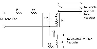
Telephone Recorder
Published:2012/12/12 20:59:00 Author:muriel | Keyword: Telephone Recorder

View full Circuit Diagram | Comments | Reading(741)
Telephone Hold Button
Published:2012/12/12 20:59:00 Author:muriel | Keyword: Telephone Hold Button


View full Circuit Diagram | Comments | Reading(1443)
Simple Phone Tap
Published:2012/12/12 20:58:00 Author:muriel | Keyword: Simple Phone Tap
View full Circuit Diagram | Comments | Reading(1194)
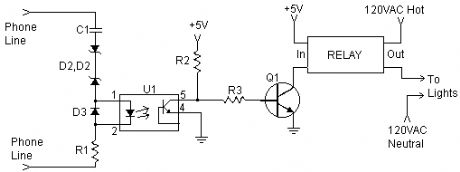
Ringing Phone Light Flasher
Published:2012/12/12 20:57:00 Author:muriel | Keyword: Ringing Phone , Light Flasher
View full Circuit Diagram | Comments | Reading(814)
Remote Telephone Ringer
Published:2012/12/12 20:56:00 Author:muriel | Keyword: Remote Telephone Ringer

View full Circuit Diagram | Comments | Reading(0)
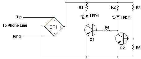
Phone Busy Indicator
Published:2012/12/12 20:55:00 Author:muriel | Keyword: Phone Busy Indicator
View full Circuit Diagram | Comments | Reading(1149)
FM Telephone Bug
Published:2012/12/12 20:55:00 Author:muriel | Keyword: FM Telephone Bug

View full Circuit Diagram | Comments | Reading(0)
The connection schematic block circuit diagram of UC3907 and external circuit
Published:2012/12/12 3:27:00 Author:Ecco | Keyword: connection , external circuit
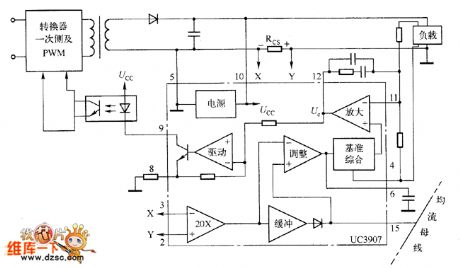
Current signal is sampling by an external shunt, RCS is generally connected with return branch in series, and it is sent to current amplifier by pin 2 and pin 3, the output voltage of the power module input uses by 11 feet and 4 feet differential signal, and it is superimposed with circulation.
(View)
View full Circuit Diagram | Comments | Reading(642)
82C250 functional block circuit diagram
Published:2012/12/12 2:58:00 Author:Ecco | Keyword: functional block
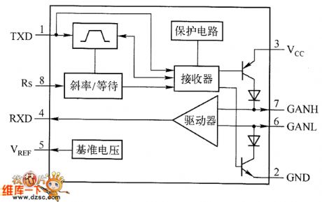
Figure 1 shows a functional block diagram between CAN controller and interface circuit 82C250 of physical bus. 82C250 is able to provide differential receive and transmit functions for bus to achieve electrical isolation between each node on the bus, and the maximum transmission rate is up to 1 Mb / s.
(View)
View full Circuit Diagram | Comments | Reading(966)
Timer alarm circuit using NE555
Published:2012/12/12 2:52:00 Author:Ecco | Keyword: Timer alarm
Timer alarm circuit using NE555 is shown as the figure.
(View)
View full Circuit Diagram | Comments | Reading(1029)
PWM inverter over-current protection circuit diagram
Published:2012/12/12 2:51:00 Author:Ecco | Keyword: PWM inverter , over-current protection
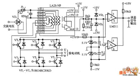
It can prevent IGBT or MOSFET output stage from being damaged by large current flowing. The maximum current is 23A when the motor is overcurrent, and the overcurrent needs 3μs flowing to protection circuit.
(View)
View full Circuit Diagram | Comments | Reading(2568)
ICL8043 dual JFET input op amp and its main characteristics
Published:2012/12/12 2:32:00 Author:Ecco | Keyword: dual JFET , input op amp, main characteristics

Input offset voltage is 10mV ; temperature drift is 75μV / ℃; bias current is 2pA ; Gain Bandwidth Product GB = 1MHz; conversion rate is 6V/μs ; Current consumption is 4.5mA ; power supply is ± 18V; differential input voltage is ± 30V ; common-mode input voltage is ± 15V; power consumption is 500mW.
(View)
View full Circuit Diagram | Comments | Reading(1182)
| Pages:244/2234 At 20241242243244245246247248249250251252253254255256257258259260Under 20 |
Circuit Categories
power supply circuit
Amplifier Circuit
Basic Circuit
LED and Light Circuit
Sensor Circuit
Signal Processing
Electrical Equipment Circuit
Control Circuit
Remote Control Circuit
A/D-D/A Converter Circuit
Audio Circuit
Measuring and Test Circuit
Communication Circuit
Computer-Related Circuit
555 Circuit
Automotive Circuit
Repairing Circuit