
Circuit Diagram
Index 132
TDA7056 3W BTL Mono Audio Power Amplifier circuit diagram
Published:2013/3/28 4:02:00 Author:Ecco | Keyword: 3W , BTL, Mono , Audio Power Amplifier
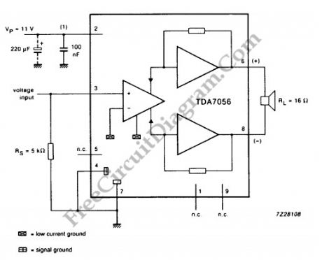
For mono output amplifier application, TDA7056 IC can be your option. Compact but powerful, this integrated circuit is contained in a 9 pin medium power package. This device is designed for battery fed portable equipments such as mono recorders, radios and television. To attract the market, TDA7056 has many features such as low power consumption. For more reliable operation, TDA7056 also has short circuit proof and ESD (Electro Static Discharge) protected on all pins. Designing application with this IC should be easy since no external components is needed. To make sure you’ll love this chip, this device also has no switch on/off clicks. Overall, TDA7056 has good stability.
(View)
View full Circuit Diagram | Comments | Reading(3208)
The square Root Mode for AD532 Analog Processor
Published:2013/3/28 4:00:00 Author:Ecco | Keyword: Square Root Mode, Analog Processor

The following schematic diagram shows us about the connections for square root mode for ADS532 analog processor chip. Similar to the division mode, the multiplier cell is connected in the feedback of the op amp by connecting the output back to both the X and Y inputs. To prevent latch up as Zi approaches 0 Volts, the diode D1 is connected. The Vov adjustment is made with Zin = +0.1 V dc in this case, adjusting Vos to obtain -1.0 V dc in the output, Vout =-√(10 VZ). Gain (S.F) and offset (Xo) adjustments are recommended for optimum performance.
(View)
View full Circuit Diagram | Comments | Reading(730)
The instrumentation Amplifier with CMRR Calibration
Published:2013/3/28 3:59:00 Author:Ecco | Keyword: Instrumentation Amplifier , CMRR Calibration
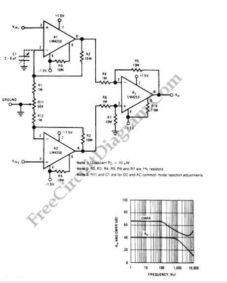
Common mode rejection ratio (CMMR) is one parameter that specify the instrumentation performance. LM4250 is high performance op-amp which is characterized by very low power consumption. With special arrangement as shown in the following schematic diagram, the instrumentation amplifier circuit will be featured with calibration to maximize the CMMR performance.
(View)
View full Circuit Diagram | Comments | Reading(1294)
Digital Encoder Circuit diagram Using Stepper Motor
Published:2013/3/28 3:57:00 Author:Ecco | Keyword: Digital Encoder, Stepper Motor

Using circuit depicted in the schematic diagram below, the direction and shaft rotation of stepper motor can be seen on the LED display. Alternative to digital rotation encoder as a digital encoder input, this circuit uses a stepper motor. Here is the schematic diagram of the circuit:
(View)
View full Circuit Diagram | Comments | Reading(3330)
The selectable Voltages 6V, 9V, and 12V Linear Voltage Regulator
Published:2013/3/28 3:55:00 Author:Ecco | Keyword: Selectable Voltages, 6V, 9V, 12V, Linear Voltage Regulator

We can build a multiple voltage power supply 6, 9, and 12V (AC-DC Adapter) with the circuit shown in the following schematic diagram. Not only provide multiple voltage output with single voltage supply, this circuit add the benefit of regulating the voltage for better stability. The TIP31 transistor should be installed with proper heat-sink to prevent overheating. A transformer with rectifier diodes and filtering capacitor can be used to supply this circuit. You can use 1 A 15V transformer with 2200uF filtering capacitor for the AC to DC adapter.
(View)
View full Circuit Diagram | Comments | Reading(1246)
Sound-Activated Lamp circuit diagram (Relay/Switch)
Published:2013/3/28 3:54:00 Author:Ecco | Keyword: Sound-Activated Lamp , Relay, Switch
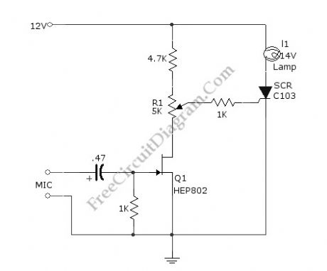
This simple circuit shown int the schematic diagram actives the switch using sound. We can use this circuit for various applications, such as automatic (sound-controlled) disco light or car’s LED light show. The Q1 amplify the audio from mic. The R1 is used to adjust the peak of signal to greater than about 0.7 volts, act as sensitivity adjuster. A certain level, the signal coming from microphone, after amplification by Q1, will trigger the SCR and light lamp I1. If we change the lamp with a relay, then we can get a sound-activated relay/switch, which can be used to control more powerful / high wattage high voltage lamps. If we use a relay, place a 1N4007 diode in parallel with the relay coil to prevent the back-emf from relay coil destroying the SCR. Here is the schematic diagram of the circuit:
(View)
View full Circuit Diagram | Comments | Reading(2322)
The Wien-Bridge Oscillator Using HA2541 Op-Amp
Published:2013/3/28 3:53:00 Author:Ecco | Keyword: Wien-Bridge Oscillator , Op-Amp
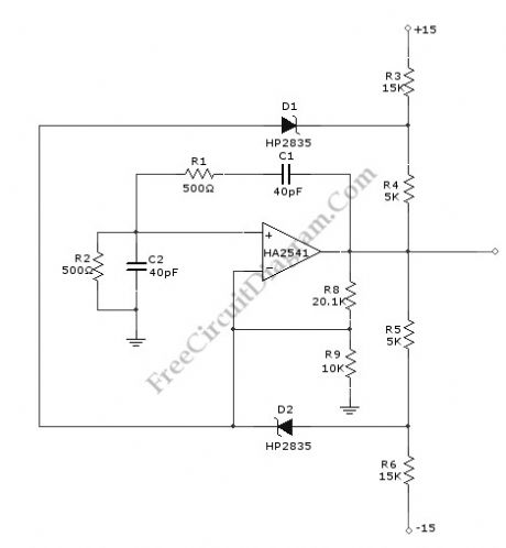
A Wien-Bridge oscillator circuit can be built from HA2541 and some basic components. This circuit can generate good-quality sine wave of 40 MHz with an upper limit of 50 MHz. The R3 through R7 and D2 and D1 provide the diode limiting for this circuit. Here is the schematic diagram of this circuit:
(View)
View full Circuit Diagram | Comments | Reading(1382)
The Ni-Cad Battery Zapper, A Rechargeable Battery Reconditioner
Published:2013/3/28 3:52:00 Author:Ecco | Keyword: Ni-Cad Battery, Zapper, A Rechargeable Battery, Reconditioner
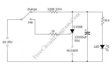
Ni-Cad (NiCd, NiCad) battery, sometimes doesn’t work as expected, gives no power and cannot be recharged. In this situation, the battery need to be reconditioned. It’ is possible that the battery is internally shorted, and we can get the battery into life again by recondition the Ni-Cad battery using a zapper circuit. This circuit restore the Ni-Cad battery from shorting by forcing a high current flow to burn the internal dirt. The current stored in the high capacitance capacitor is heavy discharged by the SCR when zapping, and the SCR is used to disconnect the battery connection when charging the capacitor. A 120 ohm 10W resistor is used to limit the current when charging the capacitor, and you have to make sure the LED’s intensity has reach the steady state before switching to zap position. After zapping the battery and switch to charge position, the charging process will take some period and indicated by the LED which will gradually increase the brightness until get stable intensity when fully charged. The power supply for this circuit can be taken from small transformer (350 mA to 1 A) with half or full wave rectifier. Here is the schematic diagram of the battery zapper circuit:
(View)
View full Circuit Diagram | Comments | Reading(2868)
The audible Logic Probe/Indicator
Published:2013/3/28 3:51:00 Author:Ecco | Keyword: Audible Logic Probe, Indicator
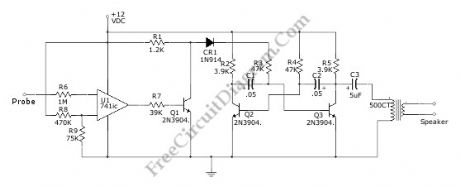
Logic indicator circuit / logic probe is used to identify logic level at any point of logic circuitry. The indicator can be visual (using LED, LCD, of 7 Segments) or auditory (using beeper or speaker). This circuit has a audible indicator, with the help of a loudspeaker to produce indication tone. Using the opamp,U1, as schmitt trigger, the Audio oscillator Q3-Q1-Q2 is isolated from TTL. Beside that, the op amp also acts as high input impedance inverter. The R8-R9 is used to set reference level at +16.6V which is a midway between low and high logic level. The Q3-Q2 will generate tone that indicate a high logic when the probe voltage is above +1.6V. If the probe voltage is below +1.6V then the OP-amp output will saturate the Q1 and disables Q3-Q2 to cut off tone. Here is the schematic diagram of the circuit:
(View)
View full Circuit Diagram | Comments | Reading(2578)
Double-Sideband Suppressed-Carrier (DSB-SC) Modulator
Published:2013/3/28 3:50:00 Author:Ecco | Keyword: Double-Sideband Suppressed-Carrier, Modulator
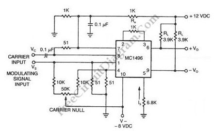
When we modulate a carrier signal with amplitude modulation, there will be four frequency components as the result. The first is the modulating signal itself, the second is the frequency carrier, the the latest two are the difference and the sum of the carrier and the modulating signal. The spectrum of these frequencies can be seen using frequency analyzer. In radio transmission, the modulating frequency components is completely filtered out since the frequency is far lower than the other three. To increase the power efficiency, double sideband suppressed carrier modulator (DSB-SC) remove the carrier frequency part, so the transmitted frequencies consist only the side bands: the sum and the difference. In the schematic diagram below, a double-sideband suppressed-carrier modulator circuit is presented. There is no carrier appear in the output because of the basic current. The Carrier amount appear in at the output can be controlled by adding offsets to the carrier differential pairs. The function of the modulation signal-AM modulation is the amplitude.
(View)
View full Circuit Diagram | Comments | Reading(3010)
The low-Drift High-Impedance JFET DC Voltmeter
Published:2013/3/28 3:49:00 Author:Ecco | Keyword: Low-Drift, High-Impedance, JFET, DC Voltmeter
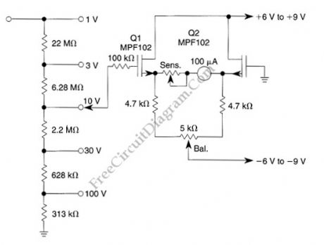
The voltmeter shown in the schematic diagram below has very high impedance. The range selector uses conventional voltage divider resistors, but since the following pre amplifier uses JFET, the divider can be designed using very high resistance series resistors. This DC voltmeter circuit also featured with low drift. This circuit uses a pair JFETs, which is configured in a balanced-bridge source-follower amplifier circuit. The Q2 and Q1 must be matched within 10% for Idss that will maintains bridge balance over temperature. Here is the schematic diagram of the circuit:
(View)
View full Circuit Diagram | Comments | Reading(1993)
The 60-dB Range Compressor For Audio
Published:2013/3/28 3:48:00 Author:Ecco | Keyword: 60-dB, Range Compressor , Audio

A compressor circuit shown in the schematic diagram below can produce consistent output of 1.4V P-P over entire 60dB range that is very useful for audio level/volume stabilization. As the main components, this circuit uses a 741 opamp and JFET. With input range of 20mV to 2oV, this circuit has delay time of 0.4s (decay time) and response time of 1.2ms (attack time). The JFET is used as voltage-controlled resistor in peak-detecting control loop of 741 opamp. Here is the schematic diagram of the circuit:
(View)
View full Circuit Diagram | Comments | Reading(945)
The TLC497CN Negative Supply Generator
Published:2013/3/28 3:47:00 Author:Ecco | Keyword: Negative Supply Generator
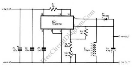
Negative supply from positive supply is needed if the circuit need both positive and negative supply while we have only positive supply. The circuit shown in the schematic diagram below is a negative supply generator, built using a TLC497CN integrated circuit. The TLC497CN is used as the main switching circuit, and it can provide negative supply of up to 150mA. With an input supply of 10V, this circuit has efficiency about 50% but it is decreased under 50% when the input voltage is 5V. This circuit use resistor R1 to protect the IC1 from damage by limiting the current at the input to IC1 because this circuit is often be fed from high current supply. To control the average output voltage, TLC497CN uses a variable clock frequency and a fixed pulse width. The timing component in the oscillator section of the PWM this circuit is capacitor C3. capacitors C2 and C1 are supply-decoupling components on the input supply.
(View)
View full Circuit Diagram | Comments | Reading(1038)
5 A Constant Voltage-Constant Current Regulator
Published:2013/3/28 3:44:00 Author:Ecco | Keyword: 5 A, Constant Voltage-Constant Current, Regulator

A constant voltage constant current (CVCS) regulator doesn’t mean a system with a constant load, since there will be no regulation in such case. What we call CVCS regulator is a regulator with two modes. The first mode is constant voltage, where the regulator trying to regulate the supply to a variable load at a constant voltage. In this mode off course the current will be variable depending on the load. The current will vary a a range that is limited to a predetermined maximum current level. When the load draw more current than this level then the regulator will switch to constant current mode, where the regulator keep the current at a fixed maximum value. Any attempt of the load to draw more current will cause the regulator to decrease the voltage as a reaction to keep it constant, so it acts like a current limiter. Here is the schematic diagram of the CVCS regulator.
(View)
View full Circuit Diagram | Comments | Reading(1617)
Voltage Controlled Variable Gain Video Amplifier
Published:2013/3/28 3:43:00 Author:Ecco | Keyword: Voltage Controlled , Variable Gain, Video Amplifier
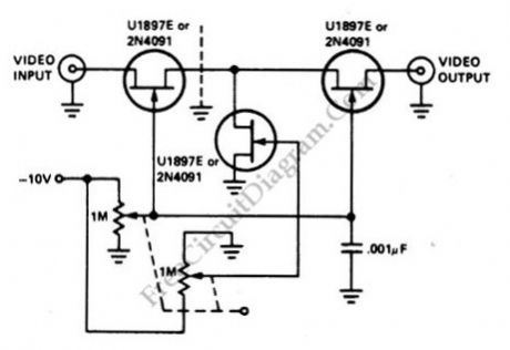
This is a video amplifier circuit featured with controllable variable gain. The control is done by adjusting the voltage of grid inputs of two FETs, which are configured as programmable voltage divider. This circuit can generate dynamic linear range attenuation up to 100 dB. This circuit still give a linear attenuation even at f=10.7MHz. You can see the control is done by a potentiometer, but you can replace with any voltage source ranging from zero to -10V, just make sure each of the two FETs is fed with different synchronized voltages. How to make this two synchronized voltages is described as follow: the first FET is fed with U1, which ranges from 0 to -10 V, and the second FET is controlled by U2, which is synchronized as (-10 – U1) V. This control voltages can be obtained from DAC (digital-to-analog converter) or a stereo potentiometer (as depicted in the diagram). You can see a grounded 0.001 uF capacitor to filter the control voltage from any glitch caused by dirty or bad potentiometer. Here is the schematic diagram of the circuit:
(View)
View full Circuit Diagram | Comments | Reading(0)
Tremolo Effect Circuit for Electric Guitar or Other Musical Instruments
Published:2013/3/28 3:42:00 Author:Ecco | Keyword: Tremolo Effect , Electric Guitar , Other Musical Instruments

Tremolo circuit is a kind of sound effect. We can see this type of effect is applied in guitar effect pedals. Tremolo effect is produced if we modulate the amplitude of an audio signal. The shape of modulating signal can vary from square wave, sawtooth, or sine. When we use a square wave, then the effect produce a knocking-like sound which might be perceived like a percussive instrument. When we use sine wave then we might perceive a kind of vibrato effect which gives impression that there is a frequency modulation, but it is actually a psycho effect because it modulate only the amplitude, not the frequency. This tremolo circuit use very low frequency (VLF) as a source of modulating signal, with frequency control by R12. The effect’s level, which is modulation depth, is controlled by R11. The amplitude modulation is obtained by controlling the gain of U1D, which has feedback path through Q1 which receives signal from U1C phase oscillator. Here is the schematic diagram of the circuit:
(View)
View full Circuit Diagram | Comments | Reading(2552)
Ultra-long period multivibrator
Published:2013/3/27 3:28:00 Author:Ecco | Keyword: Ultra-long period multivibrator
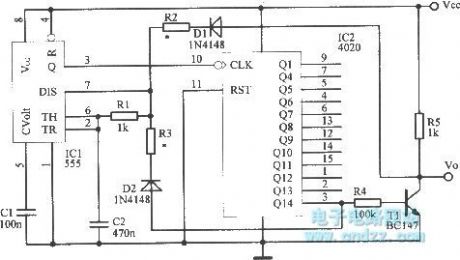
Ultra-long period multivibrator is shown as figure.
(View)
View full Circuit Diagram | Comments | Reading(976)
28.3MHz third harmonic TrL oscillator
Published:2013/3/28 1:53:00 Author:Ecco | Keyword: 28.3MHz, third harmonic , TrL oscillator
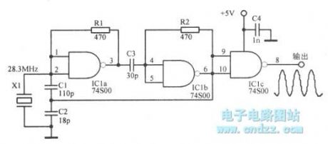
28.3MHz third harmonic TrL oscillator is shown as figure.
(View)
View full Circuit Diagram | Comments | Reading(1207)
455Hz oscillator circuit
Published:2013/3/27 3:26:00 Author:Ecco | Keyword: 455Hz , oscillator
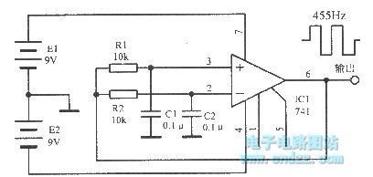
455Hz oscillator circuit is shown as figure.
(View)
View full Circuit Diagram | Comments | Reading(985)
Integrated power oscillator
Published:2013/3/27 3:27:00 Author:Ecco | Keyword: Integrated power oscillator
Integrated power oscillator is shown as figure.
(View)
View full Circuit Diagram | Comments | Reading(925)
| Pages:132/2234 At 20121122123124125126127128129130131132133134135136137138139140Under 20 |
Circuit Categories
power supply circuit
Amplifier Circuit
Basic Circuit
LED and Light Circuit
Sensor Circuit
Signal Processing
Electrical Equipment Circuit
Control Circuit
Remote Control Circuit
A/D-D/A Converter Circuit
Audio Circuit
Measuring and Test Circuit
Communication Circuit
Computer-Related Circuit
555 Circuit
Automotive Circuit
Repairing Circuit