
Circuit Diagram
Index 126
Intelligent NiCd/NiMH Battery Charger
Published:2013/5/2 21:10:00 Author:muriel | Keyword: Intelligent, NiCd/NiMH Battery , Charger

This cheap and easy to build NiCd/NiMH Battery Charger is suitable for automatically charging a wide range of batteries for many applications. Proper chargers are usually expensive and cheap chargers supplied with the original equipment often incorrectly charge the cells and dramatically shorten their life. This ‘intelligent’ charger was designed for high current and rapid charge applications such as cordless power tools and model racing cars.
(View)
View full Circuit Diagram | Comments | Reading(6211)
EL84/6BQ5 Tube Amplifier
Published:2013/4/27 22:01:00 Author:muriel | Keyword: EL84/6BQ5, Tube Amplifier

When experimenting with tube amplifiers, you might be confused about the different modes of operation, like triode or pentode mode. Here is the developed circuits which you can build small Amplifiers based on 6P14/6BQ5/EL84 easily, and the output Power of 2.6 Watts is more than enough for home use. Also,the PCB included.With this PCB you can try out the different Modes by means of Jumper Wires. (View)
View full Circuit Diagram | Comments | Reading(2538)
6SL7 SRPP / KT77 SIPP TUBE AMP
Published:2013/4/27 21:59:00 Author:muriel | Keyword: 6SL7 SRPP , KT77 SIPP, TUBE AMP

This circuit designed by Bruce and he has followed up his “OddWatt” project (EL84/6BQ5 Push-Pull) with the Oddwatt 225. The Oddwatt 225 is a scalable tube amplifier which will work with a number of octal tubes. In this build the driver stage is an SRPP with 6SL7 tubes and the output stage is a Class A UL SIPP with KT77 tubes. LM317 Regulators are used for the cathode CCS. (View)
View full Circuit Diagram | Comments | Reading(2988)
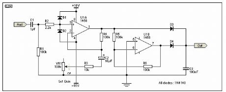
Simple Full Wave Rectifier and Preamp
Published:2013/4/26 1:48:00 Author:muriel | Keyword: Simple Full Wave, Rectifier and Preamp
View full Circuit Diagram | Comments | Reading(1359)
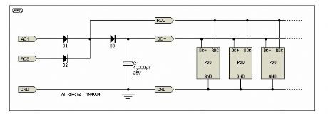
Power Supply Circuit (Two 15V AC Windings - 15-0-15)
Published:2013/4/26 1:48:00 Author:muriel | Keyword: Power Supply Circuit, Two 15V , AC Windings , 15-0-15
View full Circuit Diagram | Comments | Reading(1288)
Power Supply Circuit (Single 15V AC Winding)
Published:2013/4/26 1:47:00 Author:muriel | Keyword: Power Supply Circuit, Single 15V, AC Winding

View full Circuit Diagram | Comments | Reading(980)
LED Audio VU Meter
Published:2013/4/26 1:37:00 Author:muriel | Keyword: LED , Audio , VU Meter

View full Circuit Diagram | Comments | Reading(2117)
Stereo VU Meter
Published:2013/4/26 1:36:00 Author:muriel | Keyword: Stereo VU Meter
This is a STEREO LED LEVEL METER. It’s the cheapest and best bar graph display available and best of all, it uses readily available components.You only need a handful of LEDs, 22 transistors, some resistors, diodes and a set of electros – it doesn’t require any chips. (View)
View full Circuit Diagram | Comments | Reading(2049)
CMoy Pocket Amplifier
Published:2013/4/26 1:33:00 Author:muriel | Keyword: CMoy Pocket Amplifier
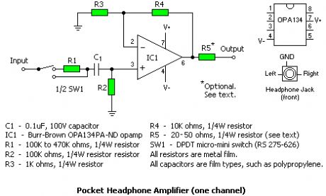
This is a very simple headphone amplifier designed by CMoy.Each channel uses a single Burr-Brown OPA134 opamp in a non-inverting configuration. It has adequate current capability to drive most headphones without an output stage.The amplifier is ideal as a booster for power-conserving stereo sources such as portable CD players and for interfacing with passive EQ networks such as tone controls or a headphone acoustic simulator. (View)
View full Circuit Diagram | Comments | Reading(2406)
Class A Headphone Amplifier
Published:2013/4/26 1:32:00 Author:muriel | Keyword: Class A , Headphone Amplifier
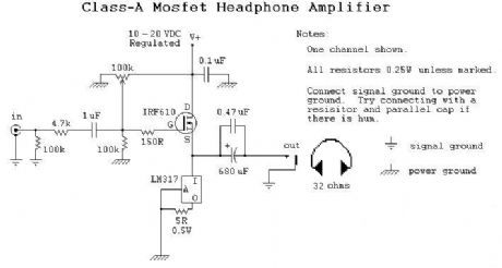
This is a simple do-it-yourself (DIY) headphone amplifier project that is fashioned primarily after the Class A MOSFET Headphone Driver project by Greg Szekeres and to some extent Mark’s DIY Class A 2SK1058 MOSFET Amplifier Project. The amplifier concept is simple and follows a typical single-ended class A circuit utilizing an active constant current source (CCS) in place of a passive resistor. A CCS doubles the efficiency of the circuit over that where a passive load resistor is used, bringing it to a maximum of 25%. (View)
View full Circuit Diagram | Comments | Reading(3511)
PPA headphone amplifier
Published:2013/4/26 1:29:00 Author:muriel | Keyword: PPA headphone amplifier

The PPA is a high-end headphone amplifier that works for both stationary and “transportable” amplifiers. There is a high-capacity fast-charging NiMH battery supply available, allowing excellent sonics without sacrificing run time despite the PPA amp’s hunger for power. While only the most dedicated audiophile would take it jogging with their iPod, this combination makes for a fine travel amplifier.
(View)
View full Circuit Diagram | Comments | Reading(2114)
2-20 Watt Stereo Audio Power Amplifier by LM1875
Published:2013/4/26 1:21:00 Author:muriel | Keyword: 2-20 Watt , Stereo, Audio, Power Amplifier , LM1875

There are many instances where a simple and reliable power amplifier is needed - rear and centre channel speakers for surround-sound, beefing up the PC speakers, low powered tweeter amplifier, etc. For those who want to build their own 'Gainclone' amplifier, this will certainly do the job :-)
This project (unlike most of the others, but in a similar vein to Project 19) is based almost directly on the typical application circuit in the National Semiconductor specification sheet. You can also use the TDA2050 (from SGS-Thompson), which has almost identical performance and (remarkably) the same pinouts! As it turns out, the amp in the NS application circuit is pretty good, as is the (very similar) one from SGS. The amp is also remarkably simple to build - if you have a PCB! These ICs are a cow to wire on Veroboard - it is possible, but results are unpredictable.
Figure 1 shows the schematic - this is almost the same as in the application note (redrawn), and with added RF protection at the input. Note that the speaker must return to the central 'star' earth (ground) point. If connected to the amplifier's earth bus, you will get oscillation and/or poor distortion performance.
Voltage gain is 27dB as shown, but this can be changed by using a different value resistor for the feedback path (R4, currently 22k, between pins 2 and 4). The amplifier must not be operated at any gain less than 10 (20dB) as set by R4 and R5, as it will oscillate. In some cases, an inductor may be needed in series with the output to prevent instability with capacitive loads (10 turns of 0.5mm wire wound around a 10 Ohm 1W resistor). The most common capacitive load is the speaker cable itself, and 'audiophile' leads are often worse than standard grade cables in this respect.
The 1 Ohm resistor (R6) should be a 1W or 0.5W type, and all others should be 1/4W 1% metal film (as I always recommend). All electrolytic capacitors should be rated at 50V if at all possible, and the 100nF (0.1uF) caps for the supplies should be as close as possible to the IC to prevent oscillation. C1 should be a bipolar (non-polarised) electrolytic, or may be plastic film if you prefer.
The supply voltage should be about ±25 Volts at full load, which will let this little guy provide a maximum of 25 Watts (rated minimum output at 25°C). To enable maximum power, it is important to get the lowest possible case to heatsink thermal resistance. This will be achieved by mounting with no insulating mica washer, but be warned that the heatsink will be at the -ve supply voltage and will have to be insulated from the chassis. For more info on reducing thermal resistance, read the article on the design of heatsinks - the same principles can be applied to ICs - even running in parallel. I haven't tried it with this unit, but it is possible by using a low resistance in series with the outputs to balance the load.
Note that the supply voltage must not exceed ±30V at any time - this is the absolute maximum voltage rating for the LM1875. Note that the TDA2050 is rated for a maximum of ±25V.
Figure 2 shows the pinouts for the LM1875, and it should be noted that the pins on this device are staggered to allow adequate sized PCB tracks to be run to the IC pins.
The PCB for this amp is for a stereo amplifier, is single sided, and supply fuses are located on the PCB. The entire stereo board including four fuses is 115mm x 40mm (i.e. really small). The heatsink needs to be bigger than you might expect, largely because of the relatively high thermal resistance of the TO-220 case. National recommend that the heatsink should be no smaller than 1.2°C / Watt (it is actually suggested that the heatsink be 0.6°C / W, but this is a very large heatsink indeed, and is not necessary for normal audio into reasonably well behaved loads.
Never operate these ICs with no heatsink, even without any load connected. The quiescent dissipation will cause them to overheat very quickly, and may damage the internal circuitry.
Output power is rated at 20W per channel, but with music signals you will probably be able to get a peak power of about 25W into an 8 ohm load. Refer to the data sheet (see link below) for the full specification on the IC. Note that the TDA spec sheet claims 50W, but this is overly optimistic and cannot be achieved in practice.
(View)
View full Circuit Diagram | Comments | Reading(2788)
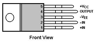
LM3886 60 Watt Amplifier
Published:2013/4/26 1:19:00 Author:muriel | Keyword: LM3886, 60 Watt, Amplifier

This is one of the stronger amps. It supports stand-by and mute modes. The schematic is rather complicated, because there are some additional devices in the feedback and there are filters both on the input and on the output. (View)
View full Circuit Diagram | Comments | Reading(2436)
Butterworth filter has adjustable group delay
Published:2013/4/18 3:00:00 Author:muriel | Keyword: Butterworth filter, adjustable group , delay
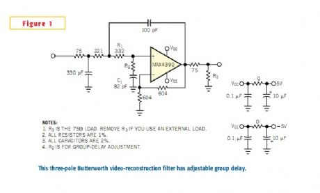
This Sallen-Key realization of a 5.25-MHz, three-pole Butterworth filter has a gain of 2V/V and can drive 75Ω back-terminated coax with an overall gain of 1 .It can used to reconstruct component-video (Y, Pb, Pr) and RGB signals, this filter has an insertion loss greater than 20 db at 13.5 MHz and greater than 40 db at 27 MHz . Like the antialiasing filter before an ADC, this filter removes the higher frequency replicas of a signal following a DAC. To preserve quality in the video waveform, you should minimize group-delay variations in the filter and any group-delay differential between filters. (View)
View full Circuit Diagram | Comments | Reading(1272)
Voltage Controlled Panner
Published:2013/4/18 2:02:00 Author:muriel | Keyword: Voltage Controlled , Panner

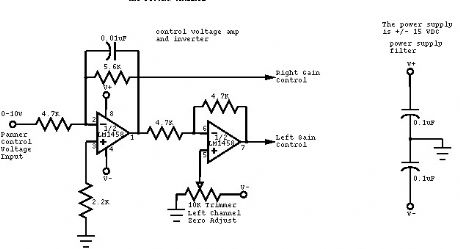
This circuit is used to convert a mono audio signal into a stereo signal that can be panned between the left and right channel by a 0-10V control signal, it is intended for analog synthesizer systems.
(View)
View full Circuit Diagram | Comments | Reading(2332)
Audio / Signal Processing
Published:2013/4/18 1:58:00 Author:muriel | Keyword: Audio, Signal , Processing

This Sallen-Key realization of a 5.25-MHz, three-pole Butterworth filter has a gain of 2V/V and can drive 75Ω back-terminated coax with an overall gain of 1 .It can used to reconstruct component-video (Y, Pb, Pr) and RGB signals, this filter has an insertion loss greater than 20 db at 13.5 MHz and greater than 40 db at 27 MHz . Like the antialiasing filter before an ADC, this filter removes the higher frequency replicas of a signal following a DAC. To preserve quality in the video waveform, you should minimize group-delay variations in the filter and any group-delay differential between filters.source (View)
View full Circuit Diagram | Comments | Reading(1011)
Doorknob Proximity Alarm for wooden door
Published:2013/4/18 1:57:00 Author:muriel | Keyword: Doorknob Proximity Alarm, wooden door
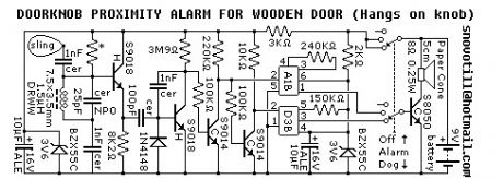
Reverse engineered circuit diagram of a popular retail doorknob alarm. It contains a small transmitter and the doorknob acts as an antenna so it will not work on a metal door. When a person comes close to the doorknob this loads down the oscillator and the alarm sounds. The proximity sensor circuitry is perfectly capable of driving 74HCT series CMOS logic in place of of the sound effect IC's shown in the circuit diagram.
(View)
View full Circuit Diagram | Comments | Reading(1316)
Electronic combination lock with PIC Microcontroller
Published:2013/4/18 1:56:00 Author:muriel | Keyword: Electronic combination lock, PIC Microcontroller
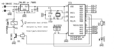
This is my electronic combination lock to use with an outdoor gate. The functionality is implemented in software. It turns on a relay (usually to open a door) for a few seconds if someone enters the valid code. Alternatively, it works as an ON/OFF switch, which toggles the relay each time the code is entered. This relay can operate a power-to-open type electric strike with a shorting contact or a power-to-hold type electromagnetic lock with a breaking contact (we need the relay because these locks usually work with AC, not DC). The code can be changed any time after entering the current code.
Current consumption of the circuit is low, because the PIC sleeps most of the time, and wakes up only for processing key presses. If you don't have a crystal, you can use the RC oscillator of the PIC16F84 as well, just check the PIC datasheets for details on oscillator configurations. The 16F628 already contains an internal RC oscillator, so no crystal is needed.
(View)
View full Circuit Diagram | Comments | Reading(1847)
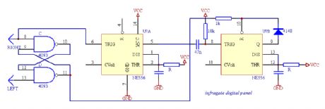
Infrared gate sensor
Published:2013/4/18 1:54:00 Author:muriel | Keyword: Infrared gate, sensor

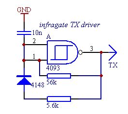

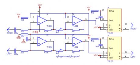
This is an infrared gate with two sensors planned to use in the wall in the way behind a door. It can be applied in a toilet to keep track of that someone is inside exceeding a certain amount of time. After that time elapsed, the circuit triggers the digital output wich can turn on a ventillator. The time period the output is turned on can be separately controlled by a second timer.
If you plan to build this circuit, beware that you may have lots of difficulties though the schematic may seem simple. The construction of the circit requires some amount of equipment like an oscilloscope and a DVM, too. Without them, the device will do weird things you wouldn't expect, and even if it is correctly put together, you must adjust it with care both mechanically in its final place and electronically with the help of an oscilloscope. Only if you want to span about less than 20-30 inches with the infra diodes can forget about this calibration. Alternatively you can take ideas from this construction.
The device consists of several parts, the most critical one is the panel with the infra LEDs. I tried to use several receiver transistors, but best result was given by infra receiver diodes used in TV remote control receivers. The receiver diodes must be properly shielded from the transmitter LED(s) otherwise the infra light will surely drive the receiver with a large enough signal. These photodiodes should only see infrared light coming from the mirror. The two very sensitive receiver parts should also be isolated from the transmitter electrically or the TX signal will get across the wires to the RX lines, which results the same effect as weak optical shielding. Use metal shielding around the receiver amplifiers where possible. The infrared transmitter LEDs should be close in wavelength to the max. sensitivity band of the receivers. You can experiment with using more LEDs and more current testing several resistor values, but don't exceed the 500 mA current limit flowing on the diodes or they will burn out. Do not shield the transmitters, allow the maximum amount of infralight to reach the mirror to extend the possible range.
Update: The TTL IC called '74123' is actually a 74HC123, and is used out of the specifications - although it is rated up to 7VDC supply voltage as absolute maximum, in this project it is powered from VCC=9-12VDC without problems. I am ashamed of neglecting such an important aspect.
To start testing the infra LED panel, you wil need the infragate amplifier panel and the small transmiter driver. The TX driver will generate the digital signal for the LED driver on the LED panel. The digital signal is 1:10 on/off to achive good performance with lower power dissipation on the LEDs. Connect GND, VCC planes and LEFT, RIGHT wires of the LED panel with the amplifier panel, and drive the TX line from the TX driver. Now you are able to start testing and calibrating the analogue part of the circuit. If everything is ok, holding a mirror in front of the LED panel will reflect enough signal to overdrive the amplifier and you can check the output on the OPA 1, 7 pins with an oscilloscope. Taking the mirror farther on will result a weakening signal on the amplifier output. Set the orientation of the diodes to be able to get the maximum signal amplitude on the oscilloscope screen. This is the heaviest part of the work, don't deal too much with it until the complete circuit is not built. Just adjust a static state of the construction to give the maximum signal amplitude on the output when nothing is between the diodes and the mirror and give a small noise only when the line of sight is covered. If you are ready with it, you can adjust the schmitt triggers built of the other two OPA parts to generate TTL pulses when the analog signal is at its maximum and stay on the same DC level when the received signal is missing.
It is also important to protect the receiver diodes from direct light as natural light will weaken the sensitivity of the diodes, and lamps will transform the 50/60 Hz modulation present in the line power. Small noise is not problem, but the received signal from the TX generator should be stronger to be able to detect it. After the ST adjustments, connect LEDs to the 74123's TTL outputs through proper value resistors. The 74123 here is used as a demodulator. If there is a periodic signal change on the input, the output will be high, while if there is no activity on the input for a given period of time, the output falls low. When you cover the line of sight of one receiver diode, the corresponding LED turns off. There should not be any flickering in the turning on/off, the output should immediately respond to the change without blinking.
If still everything is correctly working at this point, the remaining digital circuit is the easy part of the work. The outputs of the previous circuit (LEFT, RIGHT) directly connect to the remaining part. The RS memory built from two NAND gates remembers the way of the last movement direction, so if someone is in or not. If you experience problems, connect another LED to pin 10 of the RS and check if this part does what it should. If there was any activity in the past minutes, the first timer is running, but it can only trigger the second timer part, if someone is still inside. The diode from the second timer output prevents resetting itself before the timing period is over in case of another movement. For a 1 minute timing (first timer) R=470k C=100u can be used, the second part would use R=1.5M C=470u for about a 15 minute timing (t=1.1RC). The output of the second timer (pin 9) can drive a relay activating the ventillator.
(View)
View full Circuit Diagram | Comments | Reading(2019)
The improved differential circuit diagram
Published:2013/4/11 1:45:00 Author:Ecco | Keyword: improved differential
The improved differential circuit diagram is shown as figure.
(View)
View full Circuit Diagram | Comments | Reading(818)
| Pages:126/2234 At 20121122123124125126127128129130131132133134135136137138139140Under 20 |
Circuit Categories
power supply circuit
Amplifier Circuit
Basic Circuit
LED and Light Circuit
Sensor Circuit
Signal Processing
Electrical Equipment Circuit
Control Circuit
Remote Control Circuit
A/D-D/A Converter Circuit
Audio Circuit
Measuring and Test Circuit
Communication Circuit
Computer-Related Circuit
555 Circuit
Automotive Circuit
Repairing Circuit