
Index 135
PUT_BATTERY_CHARGER
Published:2009/7/6 4:25:00 Author:May
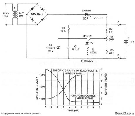
A short-circuit-proof battery charger will provide an average charging current of about 8 A to a 12-V lead/acid storage battery. The charger circuit has an additional advantage; it will not function nor will it be damaged by improperly connecting the battery to the circuit. With 115 V at the input, the circuit commences to function when the battery is properly attached. The battery provides the current to charge the timing capacitor C1 used in the PUT relaxation oscillator. When C1 charges to the peak point voltage of the PUT, the PUT fires turning the SCR on,which in turn applies charging current to the battery. As the battery charges, the battery voltage increases slightly which increases the peak point voltage of the PUT.This means that C1 has to charge to a slightly higher voltage to fire the PUT. The voltage on C1 increases until the zener voltage of Dl is reached, which clamps the voltage on C1, and thus prevents the PUT oscillator from oscillating and charging ceases. The maximum battery voltage is set by potentiometer R2 which sets the peak point firing voltage of the PUT. In the circuit shown, the charging voltage can be set from 10 V to 14 V-the lower limit being set by Dl and the upper limit by T1. (View)
View full Circuit Diagram | Comments | Reading(716)
Precision_current_source
Published:2009/7/23 20:17:00 Author:Jessie

As shown, the output current of this circuit depends on VIN and the value of R. Notice that VIN can be anything from 0 to (V- + 1 V), and V- can be -2 to -35 V. (View)
View full Circuit Diagram | Comments | Reading(0)
Fast_precision_inverter_with_50_V_μs_slcw_rate
Published:2009/7/23 20:30:00 Author:Jessie
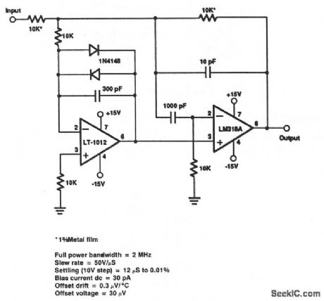
This circuit has a settling time of 12 μs to 0.1% a 10-V step input. (View)
View full Circuit Diagram | Comments | Reading(628)
CONVENTIONAL_SCHMITT_TRIGGER
Published:2009/7/23 21:07:00 Author:Jessie

Q1 is turned on when input exceeds 6.5 v, and input remains clomped at this level. As a result, input signal cannot drive additional Schmitt circuits that may have higher trigger levels.-J. Gaon, Diode and Resistor Increase Input Resistance of Schmitt, Electronics, 39:12, p 110-111. (View)
View full Circuit Diagram | Comments | Reading(655)
HUM_FREE_CASSETTE_RECORDER_SUPPLY
Published:2009/7/6 3:08:00 Author:May

Designed for tape recorder feeding into AF amplifier, to permit operation of recorder from power supply of amplifier without having hum due to positive feedback through shared ground connection. Circuit provides up to 150 mA at 7.5 V from supply ranging from 12 to 24 V. Transistors are connected as constant-currentsource in series with constant-voltage sink.Use three39-ohm resistors in parallel as 13-ohm resistor.-G. Hibbert, Avoiding Power Supply Hum, Wireless World, Oct. 1973, p 515. (View)
View full Circuit Diagram | Comments | Reading(1067)
Basic_current_to_voltage_converter
Published:2009/7/23 21:20:00 Author:Jessie
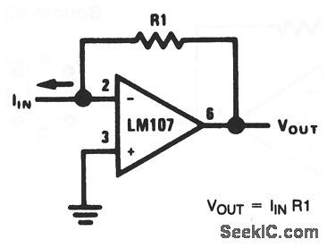
With this basic circuit, the input current is fed directly into the summing node (pin 2) and the op-amp output changes to extract the same current from the summing node through R1. The scale factor of this circuit is R1 volts per amp. That is, the output voltage is equal to the input current timesR1. The only conversion error in this circuit is Ibias, which is summed algebraically with IIN. The basic circuit can be used to measure current directly because: IIN =VOUT/R1. For example, if VOUT is 1 V (or 1000mV), and R1 is 100 Ω,IN = 10mA. (View)
View full Circuit Diagram | Comments | Reading(773)
Unity_gain_buffer
Published:2009/7/23 21:36:00 Author:Jessie

This configuration gives the highest input impedance of any op-amp circuit. Input impedance is equal to the differential input impedance multiplied by the open-loop gain, in parallel with common-mode input impedance. The gain error of this circuit is equal to the reciprocal of the open-loop gain or to the commonmode rejection, whichever is less. (View)
View full Circuit Diagram | Comments | Reading(1172)
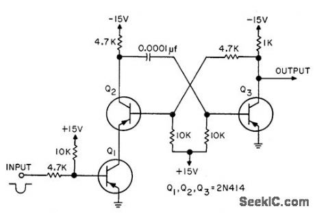
50_V_PUSH_PULL_PULSES_FOR_DIODE_BRIDGE
Published:2009/7/23 21:35:00 Author:Jessie
Schmitt trigger acts as comparator about 0 v and provides input to two pulse amplifiers. Cathode followers furnish push-pull output at low impedance necessary to drive a 6AL5 diode bridge. Permits two sampled-hold circuits to be run as memory pair in analog computer.-T. A. Brubaker, Precision Analog Memory has Extended Frequency Response, Electronics, 34:39, p 141-143. (View)
View full Circuit Diagram | Comments | Reading(1204)
TRIGGER_FOR_ANY_INPUT
Published:2009/7/23 21:27:00 Author:Jessie
D-c coupling of input permits triggering either by sine waves or pulses, independently of pulse shape or rise time.-P. L. Writer, DC Input Trigger Circuit,EEE,10:9,p 29. (View)
View full Circuit Diagram | Comments | Reading(542)
DUAL__52_V_AND___15_V
Published:2009/7/6 2:08:00 Author:May


Output voltages are equal to preset values of regulator ICs in basic arrangement shown. R1 and D1 ensure startup of LM109 when common load exists across sup-plies. D1 should be germanium or Schottky hav-ing forward voltage drop of 0.4V or less at 50 mA. D2 and D3 protect against polarity reversal of output during overloads.-C. T. Nelson, Power Distribution and Regulation Can Be Simple, Cheap and Rugged, EDNMagazine, Feb, 20, 1973, p 52-58. (View)
View full Circuit Diagram | Comments | Reading(554)
Voltage_reference
Published:2009/7/23 21:41:00 Author:Jessie
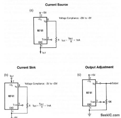
Figures 4-1A and 4-1B show an REF-01 connected as a current source, and current sink, respectively. The REF-01 trim terminal can be used to adjust the output voltage over a 10-V±300-mV range (Fig. 4-1C). This permits the output to be set at exactly 10.000 V or to 10.240 V for binary operation. (View)
View full Circuit Diagram | Comments | Reading(0)
8_A_positive_adjustable_current_regulator
Published:2009/7/23 23:55:00 Author:Jessie
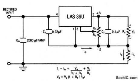
This circuit uses the LAS39U voltage-regulator IC (Fig. 7-51) as an adjustable-current regulator. Characteristics are shown in Fig. 7-50B, 7-50C, and 7-50D. (View)
View full Circuit Diagram | Comments | Reading(599)
Single_chip_supply_with_parallel_operation
Published:2009/7/23 23:00:00 Author:Jessie
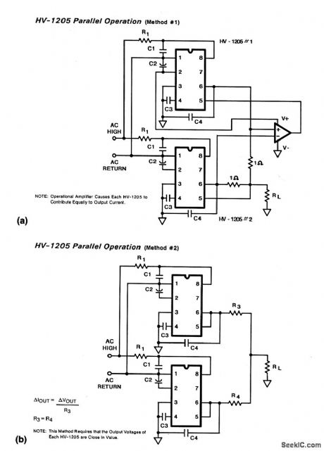
These two circuits show two HV-1205 single-chip supplies (as shown in Fig.7-6) connected in parallel to increase current capability. (View)
View full Circuit Diagram | Comments | Reading(594)
High_side_power_supplies
Published:2009/7/23 22:59:00 Author:Jessie
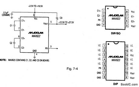
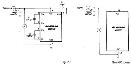
Figure 7-4 shows a MAX622 connected to generate a regulated output voltage thati s 11 V greater than the input supply voltage. The primary use is to power high-side switching and control circuits.The output current is 25 mA. with a typical qulescentcurrent of 70 μA. Figure 7-5 shows quiescent Supply current test circuits. The MAX623 has internal charge-pump capacitors.The logic level PR (power ready) output indicates when the high-side voltage reaches the proper level.MAXIM NEWRELEASES DATA Book 1992 P. 4-31 4-37. (View)
View full Circuit Diagram | Comments | Reading(696)
CURRENT_TUNED_UHF_TUNER
Published:2009/7/23 21:47:00 Author:Jessie
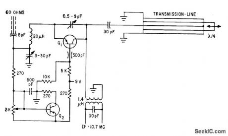
Circuit permits operation of transistors beyond rated frequency limit. Transistor is used as negative-feedback oscillator whose frequency is determined by length of coaxial line. Operation is similar to that of parametric amplifier.-U. L. Rohde, Pushing Transistors Above Their Frequency Limits, Electronics, 35:25, p 46-49. (View)
View full Circuit Diagram | Comments | Reading(568)
Dual Polarity Output Voltage Source Circuit of LM199
Published:2011/7/24 8:21:00 Author:Michel | Keyword: Output Voltage, Source Circuit

Dual polarity output benchmark voltage source circuit is as above.It outputs the benchmark voltage which is from negative to positive voltage.The LM199 heater is connected to ±15V power supply.RP1 is ten laps line potentiometer which alters its value to make the output change between +Uz~-Uz.Uz is the stability voltage in LM199 voltage regulating tube. A1 chooses LM1O8A operational amplifier and when it outputs positive voltage.A1 working condition is the same phase amplifier and A1 working condition is the inverse phase amplifier when it outputs inverse voltage. (View)
View full Circuit Diagram | Comments | Reading(670)
A_C_TO_D_C_VOLTAGE_STANDARDIZATION
Published:2009/7/23 22:03:00 Author:Jessie

High-gain d-c amplifier is used in feedback circuit to standardize ct< voltages directly to standard cell.-E. A. Gilbert, Feedback Circuits for A-C Instrument Calibration, Electronics, 33:40, p. 94-96. (View)
View full Circuit Diagram | Comments | Reading(505)
TONE_PROBE_FOR_TESTING_DIGITAL_ICs
Published:2009/7/5 23:00:00 Author:May

Circuit Notes
The tone probe uses sound to tell the status of the signal being probed. The probe's input circuit senses the condition of the signal and produces either a low-pitched tone for low-level signals (less than 0.8 V) or a high-pitched tone for high-level signals (greater than 2 V). (View)
View full Circuit Diagram | Comments | Reading(0)
Universal regulated power supply circuit diagram
Published:2011/5/10 2:24:00 Author:Rebekka | Keyword: Universal regulated power supply

View full Circuit Diagram | Comments | Reading(556)
Positive and negative output voltage tracking regulated power supply integrated circuit diagram 1
Published:2011/5/10 2:23:00 Author:Rebekka | Keyword: output voltage tracking , regulated power supply

Here is the diagramof positive and negative output voltage tracking regulated power supply integrated circuit composed of CW117, CW217 and CW317. (View)
View full Circuit Diagram | Comments | Reading(677)
| Pages:135/291 At 20121122123124125126127128129130131132133134135136137138139140Under 20 |
Circuit Categories
power supply circuit
Amplifier Circuit
Basic Circuit
LED and Light Circuit
Sensor Circuit
Signal Processing
Electrical Equipment Circuit
Control Circuit
Remote Control Circuit
A/D-D/A Converter Circuit
Audio Circuit
Measuring and Test Circuit
Communication Circuit
Computer-Related Circuit
555 Circuit
Automotive Circuit
Repairing Circuit