
Index 124
50_W_OFF_LINE_SWITCHING_POWER_SUPPLY
Published:2009/7/9 3:33:00 Author:May
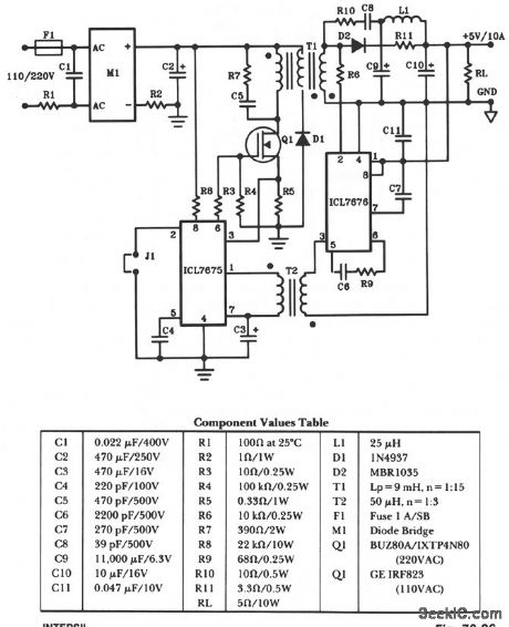
The schematic shows a 50-W power supply with a 5-V 10-A output. It is a flyback converter operating in the continuous mode. The circuit features a primary side and secondary side controller will full-protection from fault conditions such as overcurrent. After the fault condition has been removed, the power supply will enter the soft-start cycle before recommencing normal operation. (View)
View full Circuit Diagram | Comments | Reading(868)
SAFE_CONSTANT_CURRENT_SOURCE
Published:2009/7/9 3:28:00 Author:May
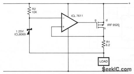
In the circuit shown, a CMOS op amp controls the current through a p-channel HEXFET power transistor to maintain a constant voltage across R1. The current is given by: 1 = VREF/R1. The advantages of this configuration are: (a) in the event of a component failure, the load current is limited by R1; and (b) the overhead voltage needed by the op amp and the HEXFET is extremely low. (View)
View full Circuit Diagram | Comments | Reading(992)
POWER_CONVERTER
Published:2009/7/9 3:20:00 Author:May
This circuit consists of an astable multivibrator driving a push-pull pair of transistors into the trans-former primary. The multivibrator frequency should equal around 1 or 2 kHz. For higher dc voltages, voltage multipliers on the secondary circuit have been used successfully to generate 10 kV from a 40-stage multiplier like the one shown. (View)
View full Circuit Diagram | Comments | Reading(1)
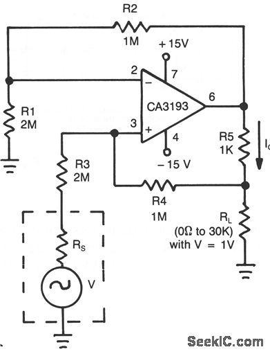
BILATERAL_CURRENT_SOURCE
Published:2009/7/9 3:19:00 Author:May


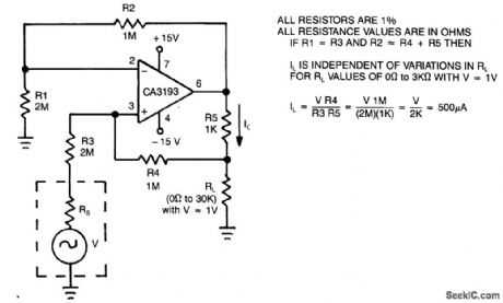
This circuit uses a CA3193 precision op amp to deliver a current independent of variations in RL. With A1 set equal to R3, and R2 approximately equal to R4 + R5, the output current, IL is:VIN (R4)/(R3) (R5). 500-μA load current is constant for load values from 0 to 3 Ω. (View)
View full Circuit Diagram | Comments | Reading(0)
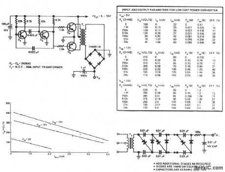
CHARGE_POOL_POWER_SUPPLY
Published:2009/7/9 3:17:00 Author:May


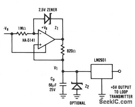
It is usually desirable to have the remote transmitter of a 4 to 20 mA current loop system powered directly from the transmission line. In some cases, this is not possible because of the high-power requirements set by the remote sensor/transmitter system. In these cases, an alternative to the separate power supply is still possible. If the remote transmitter can be operated in a pulsed mode where it is active only long enough to perform its function, then a charge pool power supply can still allow the transmitter to be powered directly by the current loop. In this circuit, constant current I1 is supplied to the charge pool capacitor, CP, by the HA-5141 (where I1 = 3 mA). The voltage V1 continues to rise until the output of the HA-5141 approaches + VS or the optional voltage limiting prodded by Z2. The LM2931 voltage regulator supplies the transmitter with a stable +5 V supply from the charge collected by CP. Available power supply current is determined by the duration, allowable voltage droop on CP, and required repetition rate. For example, if F1 is allowed to droop 4.4 V and the duration of operation is 1 ms, the available power supply current is approximately: (View)
View full Circuit Diagram | Comments | Reading(600)
VOLTAGE_CONTROLLED_CURRENT_SOURCE_WITH_GROUNDED_SOURCE_AND_LOAD
Published:2009/7/9 3:13:00 Author:May
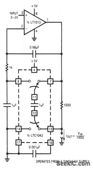
This is a simple, precise voltage-controlled current source. Bipolar supplies will permit bipolar output. Conftgurations featuring a grounded voltage-control source and a grounded load are usually more complex and depend upon several components for stability. In this circuit, accuracy and stability almost entirely depend upon the 100-Ω shunt. (View)
View full Circuit Diagram | Comments | Reading(588)
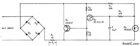
PROGRAMMABLE_POWER_SUPPLY
Published:2009/7/9 3:10:00 Author:May
Many systems require one or more relatively low-current voltage sources which can be programmed to a few predetermined levels. The circuit shown above produces positive output levels, but could be modified for negative or bipolar outputs. Q1 is the series regulator transistor, selected for the required current and power capability. R1, Q2, and Q3 form an optional short circuit protection circuit, with R1 chosen to drop about 0.7 V at the maximum output current. The compensation capacitor, C, should be chosen to keep the overshoot, when switching, to an acceptable level. (View)
View full Circuit Diagram | Comments | Reading(0)
THREE_RAIL_POWER_SUPPLY
Published:2009/7/9 3:08:00 Author:May
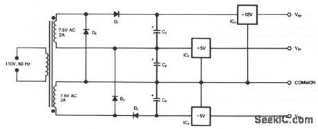
This circuit generates three supply voltages using a minimum of components. Diodes D2 and D3 perform full-wave rectification, alternately charging capacitor C2 on both halves of the ac cycle. On the other hand, diode D1 with capacitor C1, and diode D4 with capacitor C3 each perform half-wave rectification. The full- and half-wave rectification arrangement is satisfactory for modest supply currents drawn from - 5 and +12-V regulators IC3 and IC2. You can use this circuit as an auxiliary supply in an up-based instru-ment, for example, and avoid the less attractive alternatives of buying a custom-wound transformer, build-ing a more complex supply, or using a secondary winding, say 18 Vac, and wasting power in the 5-V regulators. (View)
View full Circuit Diagram | Comments | Reading(569)
GENERAL_PURPOSE_POWER_SUPPLY
Published:2009/7/9 3:03:00 Author:May


The supply 6-66 can be used for supply output voltages from 1 to 35 V. The line transformer should be selected to give about 1.4 times the desired output voltage from the positive side of ftlter capacitor C1 to ground. Potentiometer R2 sets the output voltage to the desired value by adjusting the referince input.RSC is the current limit set resistor. Its value is calculated as:For example,if the maxlmum current output is to be 1 A,RSC=0.65/1.0=0.65Ω.The 1-KΩ resistor,RS,is a light-loaded resistor designed to improve the no-load stability of the supply. (View)
View full Circuit Diagram | Comments | Reading(1400)
SIMPLE_POWER_SUPPLY
Published:2009/7/9 2:59:00 Author:May
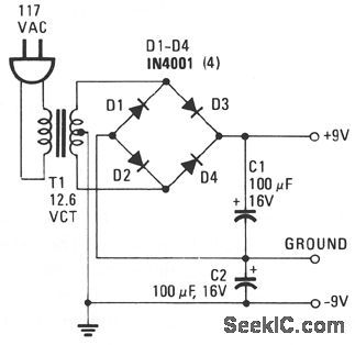
This power supply delivers plus and minus 9 V to replace two 9-V batteries. The rectifier circuit is actually two separate full-wave rectifters fed from the secondary of the transformer. One full-wave rectifier is composed of diodes D1 and D2, which develop + 9 V, and the other is composed of D3 and D4, which develop -9 V.Each diode from every pair rectifies 6.3 Vac, half the secondary voltage, and charges the associ-ated filter capacitor to the peak value of the ac waveform, 6.3 x 1.414 = 8.9 V. Eachdiode should have a PIV, Peak Inverse Voltage, rating that is at least twice the peak voltage from the transformer, 2 x 8.9 = 18 V. The 1N4001 has a PIV of 50 V. (View)
View full Circuit Diagram | Comments | Reading(1282)
12_VOC_BATTERY_OPERATED_120_VAC_POWER_SOURCE
Published:2009/7/9 2:56:00 Author:May
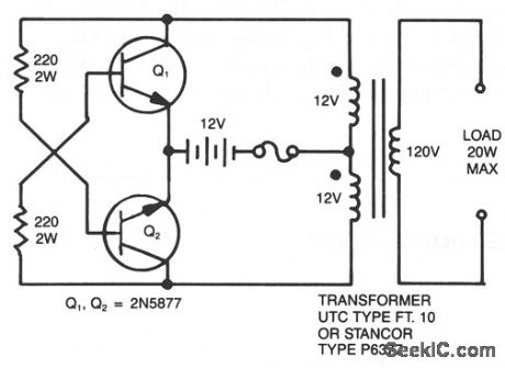


A simple 120 V: 24 V, center-tapped control transformer and four additional components can do the job. This circuit outputs a clean 200 V pk-pk square wave at 60 Hz and can supply up to 20 W. The circuit is self-starting and free-running.If Q1 is faster and has a higher gain than Q2, it will turn on first when you apply the input power and will hold Q2 off. Load current and transformer magnetizing current then flows in the upper half of the primary winding, and auto transformer action supplies the base drive until the transformer saturates. When that action occurs, Q1 loses its base drive. As it turns off, the transformer voltages reverse, turning Q2 on and repeating the cycle. The output frequency depends on the transformer iron and input voltage, but not on the load. The frequency will generally range between 50 to 60 Hz with a 60-Hz transformer and car battery or equivalent source. The output voltage depends on turns ratio and the difference between input voltage and transistor saturation voltage. For higher power, use larger transformers and transistors. This type of inverter normally is used in radios, phonographs, hand tools, shavers, and small fluorescent lamps. It will not work with reactive loads (motors) or loads with high inrush currents, such as coffee pots, frying pans, and heaters. (View)
View full Circuit Diagram | Comments | Reading(1904)
-15_V_1_A_REGULATED_POWER_SUPPLY
Published:2009/7/9 2:51:00 Author:May
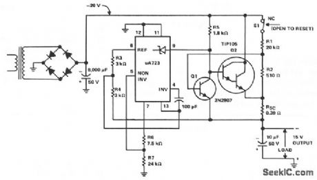
The supply receives -20 V from the rectifter/ftlter which is fed to the collector of the Darlington pnp pass transistor, a TIP105. The base drive to the TIP105 is supplied through resistor R5. The base of the TIP105 is driven from VZ terminal at pin 9, which is the anode of a 6.2-V zener diode that connects to the emitter of the μA723 output control transistor. The method of providing the positive feedback required for foldback action is shown. This technique introduces positive feedback by increased current flow through resistors R1 and R2 under short-circuit conditions. This forward biases the base-emitter junction of the 2N2907 sensing transistor, which reduces base drive to the TIP105. (View)
View full Circuit Diagram | Comments | Reading(779)
_15_V_1_A_REGULATED_POWER_SUPPLY
Published:2009/7/9 2:50:00 Author:May
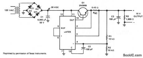
The supply receives +20 Vdc from the rectifier/filter section. This is applied to pins 11 and 12 of the μA723, as well as to the collector of the 2N3055 series-pass transistor. The output voltage is sampled through R1 and R2, providing about 7 V with respect to ground at pin 3. The reference terminal at pin 6 is tied directly to pin 5, the noninverting input of the error amplifter. For fine trimming the output voltage, a potentiometer can be installed between R1 and R2. A 100-μF capacitor from pin 13 to pin 4 furnishes gain compensation for the amplifter.Base drive to the 2N3055 pass transistor is furnished by pin 10 of the μA723. Since the desired output of the supply is 1 A, maximum current limit is set to 1.5 A by resistorRSC whose value is 0.433 Ω.A 100-μF electrolytic capacitor is used for ripple voltage reduction at the output. A 1-KΩ output resistor provides stability for the power supply under no-load conditions. The 2N3055 pass transistor must be mounted on an adequate heatsink. (View)
View full Circuit Diagram | Comments | Reading(1638)
ISOLATED_FEEDBACK_POWER_SUPPLY
Published:2009/7/9 2:37:00 Author:May

Figure 73-4 is a power supply circuit using the isolated feedback capabilities of the TL3103 for both current and voltage sensing. This supply is powered from the ac power line and has an output of 5 V at 1.5 A. Both output voltage and current are sensed and the error voltages are applied to the error amplifters of the TL594 PWM control IC. The 24-V transformer produces about 35 V at the 1000-μF filter capacitor. The 20-kHz switching frequency is set by the 6-KΩ resistor and the 0.01-μF capacitor on pins 6 and 5, respectively. The TL594 is set for push-pull operation by typing pin 13 high. The 5-V reference on pin 14 is tied to pin 15, which is the reference or the current error amplifier. The 5-V reference is also tied to pin 2 which is the reference for the output voltage error amplifier. The output voltage and current limit are set by adjustment of the 10-KΩ pots in the TL3103 error-sensing circuits. A pair of TIP31E npn transistors are used as switching transistors in a push-pull circuit. (View)
View full Circuit Diagram | Comments | Reading(2476)
O_TO_200_nA_CURRENT_SOURCE
Published:2009/7/9 2:32:00 Author:May

This circuit uses readily available parts to implement a 0-to-200-nA current source. The circuit bor-rows a PMOS transistor from the input stage of a DC4007A, which is easier to obtain than a discrete PMOS transistor. The CA3130 op amp operates as a follower so that its positive input sets the current that flows through R2. The MOSFET input stage of this op amp exhibits low-input current. The op amp must be able to produce an output voltage high enough to turn the CD4007A's internal FET off. Thus, the op amp requires a positive supply voltage of 5 V. The circuit presents an output voltage from 0 to 3 V, and R1 controls the amount of output current.
(View)
View full Circuit Diagram | Comments | Reading(1517)
SWITCHING_POWER_SUPPLY
Published:2009/7/9 2:26:00 Author:May
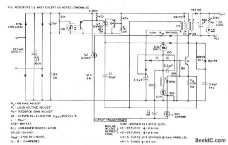
This low-voltage high-current output, switching dc power supply is running off the 220-Vac input. In this circuit, an ST2 diac relaxation oscillator, Q3, C1, and the diac, initiates conduction of the output switching transistor Q1, the on-time of which is maintained constant by a separate timing/commutation network consisting of Q2, C2, SUS, and SCR 1. The output voltage, consequently, is dependent on the duty cycle. To compensate for unwanted variations of output voltage because of input voltage or load resistance fluctuations, an H11C wired as a linear-model unilateral PNP transistor in a stable differential amplifier configuration is connected into the galvanically isolated negative-feedback loop. The loop determines the duty cycle and hence the output voltage. Of further interest in this circuit is the use of several low-current, high-voltage, 400VDRM thyristors (Q2, Q3,) which are also used as pnp remote-base transistors. Short-circuit protection is assured by coupling Q1 collector-current feedback into the turn-off circuitry via RSS. (View)
View full Circuit Diagram | Comments | Reading(0)
SCR_FIRING_ANGLE_CONTROL
Published:2009/7/20 7:43:00 Author:Jessie
Unijunction transistor trigger circuit fires scr at specific time in each half-cycle of keep average load voltage constant over line voltage range of l00 to 200 v a-c.-R. S. Krochmal and W. Weber, Controling SCR Firing Angle Regulates D-C Load Voltage, Electronics, 38:16, p 80-81. (View)
View full Circuit Diagram | Comments | Reading(2445)
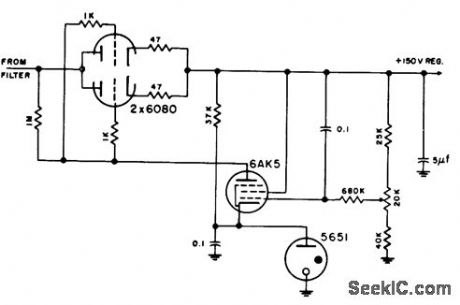
PREFERRED__150_V_D_C_REGULATOR
Published:2009/7/20 7:42:00 Author:Jessie
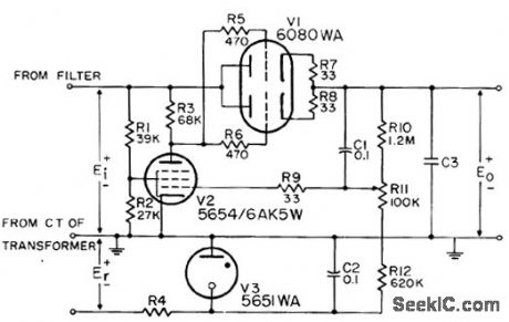
Provides 1% output voltage regulation under normal line and load variations of military equipment. Minimum value of C3 is 2 mfd. Value of R4 depends on reference voltage Er, which should be minimum of -150 v d-c. Minimum input voltage is 200 v d-c.-NBS, Handbook Preferred Circuits Navy Aero-nautical Electronic Equipment, Val. 1, Electronic Tube Circuits, 1963, PC 1, p 1-2. (View)
View full Circuit Diagram | Comments | Reading(0)
POSITIVE_REFERENCE_REGULATOR_1
Published:2009/7/20 7:40:00 Author:Jessie
Has self-contained 150-v positive reference potential for pentode regulator, but gives only marginal operation.-NBS, Handbook Preferred Circuits Navy Aeronautical Electronic Equipment, Vol. 1, Electron Tube Circuits, 1963, p N2-4. (View)
View full Circuit Diagram | Comments | Reading(638)
POSITIVE_REFERENCE_REGULATOR
Published:2009/7/20 7:39:00 Author:Jessie

Has self-contained 150-v positive reference potential for pentode regulator, but gives only marginal operation.-NBS, Handbook Preferred Circuits Navy Aeronautical Electronic Equipment, Vol. 1, Electron Tube Circuits, 1963, p N2-4. (View)
View full Circuit Diagram | Comments | Reading(575)
| Pages:124/291 At 20121122123124125126127128129130131132133134135136137138139140Under 20 |
Circuit Categories
power supply circuit
Amplifier Circuit
Basic Circuit
LED and Light Circuit
Sensor Circuit
Signal Processing
Electrical Equipment Circuit
Control Circuit
Remote Control Circuit
A/D-D/A Converter Circuit
Audio Circuit
Measuring and Test Circuit
Communication Circuit
Computer-Related Circuit
555 Circuit
Automotive Circuit
Repairing Circuit