power supply circuit
_15_V_1_A_REGULATED_POWER_SUPPLY
Published:2009/7/9 2:50:00 Author:May | From:SeekIC

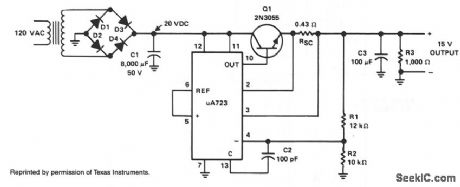
The supply receives +20 Vdc from the rectifier/filter section. This is applied to pins 11 and 12 of the μA723, as well as to the collector of the 2N3055 series-pass transistor. The output voltage is sampled through R1 and R2, providing about 7 V with respect to ground at pin 3. The reference terminal at pin 6 is tied directly to pin 5, the noninverting input of the error amplifter. For fine trimming the output voltage, a potentiometer can be installed between R1 and R2. A 100-μF capacitor from pin 13 to pin 4 furnishes gain compensation for the amplifter.Base drive to the 2N3055 pass transistor is furnished by pin 10 of the μA723. Since the desired output of the supply is 1 A, maximum current limit is set to 1.5 A by resistorRSC whose value is 0.433 Ω.A 100-μF electrolytic capacitor is used for ripple voltage reduction at the output. A 1-KΩ output resistor provides stability for the power supply under no-load conditions. The 2N3055 pass transistor must be mounted on an adequate heatsink.
Reprinted Url Of This Article:
http://www.seekic.com/circuit_diagram/Power_Supply_Circuit/_15_V_1_A_REGULATED_POWER_SUPPLY.html
Print this Page | Comments | Reading(3)

Article Categories
power supply circuit
Amplifier Circuit
Basic Circuit
LED and Light Circuit
Sensor Circuit
Signal Processing
Electrical Equipment Circuit
Control Circuit
Remote Control Circuit
A/D-D/A Converter Circuit
Audio Circuit
Measuring and Test Circuit
Communication Circuit
Computer-Related Circuit
555 Circuit
Automotive Circuit
Repairing Circuit
Code: