
Index 138
Step_up_voltage_regulator_with_voltage_dependent_oscillator
Published:2009/7/23 22:37:00 Author:Jessie
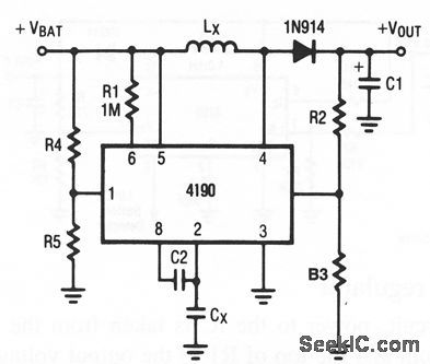
The circuit of Fig. 4-9 offers a compromise between load-current capability and output ripple (increased load current typically causes increased ripple). Component values are tailored to circuit requirements, as described for Fig.4-2, except as follows:
Typical component values are: R2= 330 kΩ, Rs=150 kΩ, Cx 100 pF, C2=100 pF. With these values, VTH is 4-1 V and Fo= 24 kHz. If the IC oscillator appears to be destabilized, or if there is excessive low-frequency ripple, look for stray capacitance at pin 7. Also, try a 100-pF to 10-nF capacitor in parallel with R2.
(View)
View full Circuit Diagram | Comments | Reading(740)
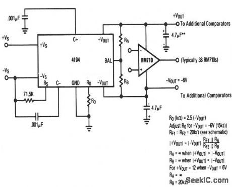
Balanced_dual_tracking_regulator_
Published:2009/7/23 22:53:00 Author:Jessie
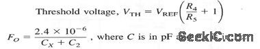
This circuit provides blanced output voltage that can be varied between±50 and ±42 mV by selection of Ro,with load currents of 200mV. This circuit is particularly useful for op-amp (chapter 10) applications, (View)
View full Circuit Diagram | Comments | Reading(747)
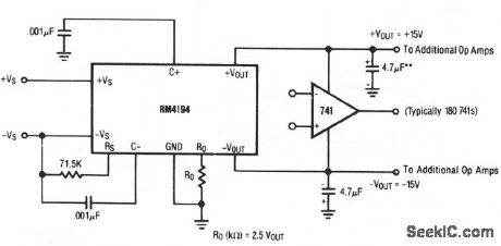
Dual_preregulated_off_line_linear_supply
Published:2009/7/23 22:53:00 Author:Jessie
This circuit provides a +12-V and a -12-V output, both of which are capable of delivering 1.5 A. (View)
View full Circuit Diagram | Comments | Reading(554)
High_side_MOSPET_driver
Published:2009/7/23 22:53:00 Author:Jessie
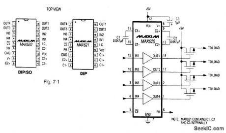
Figure 7-1 shows a MAX620 connected to power high-side switching and control circuits. The charge pump delivers a regulated output voltage that is 11 V higher than VCC to the drivers. In turn, the drivers translate a TTL/CMOS input signal to a noninverted output that swings from ground to the high-side voltage. The continuous driver-output current is 25 mA, with a typical quiescent current of 70 μA. The MAX620 requires three external charge-pump capacitors. The MAX621 has internal capacitors. MAXIM NEW RELEASES DATA Book, 1992, P. 4-19. (View)
View full Circuit Diagram | Comments | Reading(888)
Adjustable_off_line_linear_supply
Published:2009/7/23 22:50:00 Author:Jessie
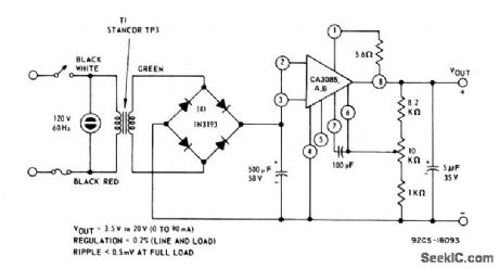
This circuit provides an output adjustable from 3.5 to 20 V, with a 90-mA load. Line and load regulation is 0.2%. Full-load ripple is 0.3 mV. (View)
View full Circuit Diagram | Comments | Reading(825)
Unbalanced_dual_tracking_regulator
Published:2009/7/23 22:45:00 Author:Jessie
This circuit provides unbalanced output voltages that can be varied between ±50 mV and ±42 V by the selection of Ro, with load currents of ±200 mV This circuit is particularly useful for comparator applications. (View)
View full Circuit Diagram | Comments | Reading(708)
Simple_5_V_fixed_regulator
Published:2009/7/23 23:16:00 Author:Jessie
This simple circuit accepts line voltages from 7 to 35V, and produces a regulated 5-V output at 1.5A. C1 is added to prevent oscillation. (View)
View full Circuit Diagram | Comments | Reading(553)
Peak_clipping_ac_voltage_regulator
Published:2009/7/23 23:16:00 Author:Jessie

This circuit uses two linear regulators to clip a 12-Vac input signal to a precise 6 Vpp at 1 A. Symmetry of the output signal depends on precise selection of the 120/480 resistors. (View)
View full Circuit Diagram | Comments | Reading(974)
Wide_range_V_F_converter
Published:2009/7/23 23:15:00 Author:Jessie

Fig. 12-3 This circuit features 1-Hz to 1.25-MHz operation with 0.05% linearity, and a typical temperature coefficient of 20 ppm/℃. Notice that in the lower frequency ranges, currents at the junction of the 330-pF capacitor and the Q1 collector are small and board leakage can cause jitter. If so, mount the capacitor, Q1, and the inverter input connection on a teflon standoff, using short connections. To trim, apply +5.000 V and adjust the 1.25-MHz trim for 1.2500-MHz Output. Linear Technology Linear Applications Handbook 1990 p AN9-13.
(View)
View full Circuit Diagram | Comments | Reading(641)
12_V_battery_charger
Published:2009/7/23 23:15:00 Author:Jessie

This circuit provides for a quick charge of 12-V gelled-electrolyte lead-acid batteries, and shuts off at full charge. The LED turns on when the battery is fully charged. (View)
View full Circuit Diagram | Comments | Reading(3249)
Quartz_stabilized_V_F_converter
Published:2009/7/23 23:31:00 Author:Jessie

Fig. 12-9 This circuit does not require an external clock (as does the circuit of Fig. 12-6) but uses a 100-kHz crystal to provide 0.005% linearity with 5 ppm/℃ drift, and a range of 1 Hz to 10 kHz. To trim, apply 10.000 V and adjust the 10-kHz trim for 10.000 kHz. Linear Technology Linear Applications Handbook, 1990 p AN14-6. (View)
View full Circuit Diagram | Comments | Reading(683)
_5_A_positive_adjustable_voltage_regulator
Published:2009/7/23 23:31:00 Author:Jessie
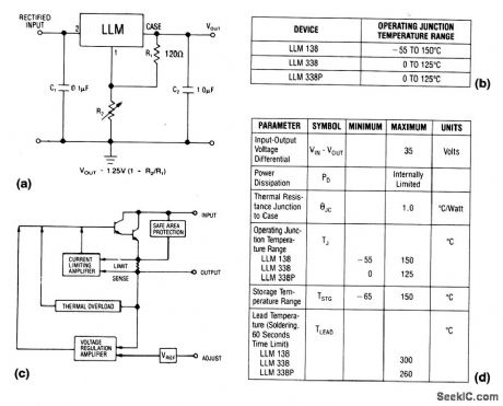
The LLM is a three-terminal adjustable regulator IC with an output range from +1.2 to +32V, with the output voltage set by two external resistors. Because the regulator is floating, higher output voltages can be obtained as long as the maximum input-output voltage differential is not exceeded. Characteristics are shown in Fig. 7-36B, 7-36C, and 7-36D. (View)
View full Circuit Diagram | Comments | Reading(670)
15_A_positive_adjustable_current_regulator
Published:2009/7/23 23:30:00 Author:Jessie
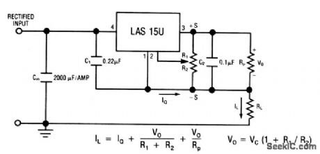
This circuit uses the LAS15AU voltage-regulator IC (Fig. 7-33) as an adjustable-current regulator. Characteristics are shown in Fig. 7-32B, 7-32C, and 7-32D. (View)
View full Circuit Diagram | Comments | Reading(562)
15_A_positive_fixed_current_regulator
Published:2009/7/23 23:30:00 Author:Jessie
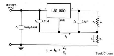
This circuit uses the LAS1500 series voltage regulator (Fig.7-32A) as a fixed-current regulator. Characteristics are shown in Fig. 7-32B, 7-32C, and 7-32D. (View)
View full Circuit Diagram | Comments | Reading(515)
Simple_adjustable_linear_regulator
Published:2009/7/23 23:03:00 Author:Jessie
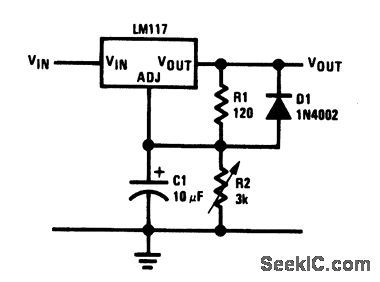
This circuit has a 1.2- to 25-V output range, set by R2. C1 improve ripple rejection. D1 prevents power surges (over 25-V output) from damaging capacitors. (View)
View full Circuit Diagram | Comments | Reading(609)
Worldwide_single_chip_supply_with_parallel_operation
Published:2009/7/23 23:03:00 Author:Jessie
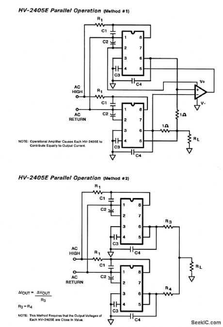
These two circuits show two HV-2405 single-chip supplies (Fig. 7-8) connected in parallel to increase current capability. (View)
View full Circuit Diagram | Comments | Reading(645)
Smgle_load_switch
Published:2009/7/23 23:03:00 Author:Jessie
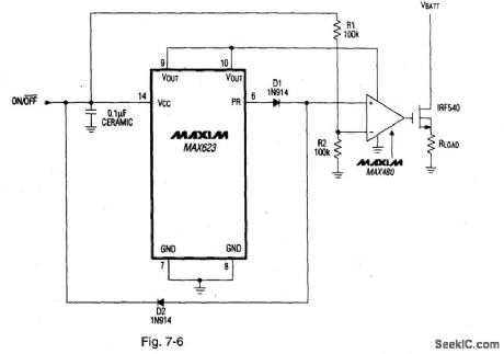
Figure 7-6 shows a MAX623 connected as a comparator-switch. The switch is turned on by applying VBATT to the ON/OFF input and turned off by pulling the input to ground. MAXIM NEW RELEASES DATA Book, 1992, P. 4-38.
(View)
View full Circuit Diagram | Comments | Reading(918)
Worldwide_single_chip_supply
Published:2009/7/23 23:02:00 Author:Jessie
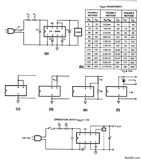
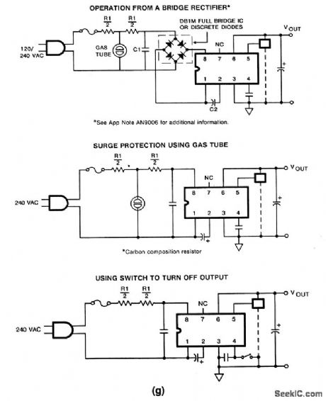
The HV-2405 converts ac into regulated dc, as described for the HV-1205 (Figs. 7-6 and 7-7), except that the HV-2405 operates from either 120 or 240 Vac (without special connections or a changeover switch). Recommended values for components shown in Figs. 7-8C through 7-8G are as follows: fuse F1=1/2 A, 2AG; R1=150 g; C1=0.05 μF, ac rated; MOV=V130LA20, or gas tube, which arcs at less than 500 V for 240 V use; C2, C3, C4, R2, RA, RB, and VZ are the same as for HV-1205. The HV-2405 does not provide isolation from the line (both ground and ac return are above ground). (View)
View full Circuit Diagram | Comments | Reading(846)
Positive_and_negative_voltage_converter_1
Published:2009/7/23 23:07:00 Author:Jessie
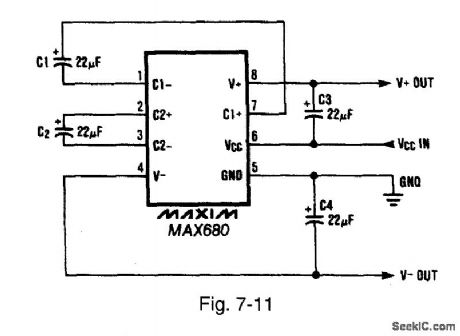
Figure 7-11 shows a MAX680 used as a positive and negative voltage converter. Capacitors C1 and C3 must be rated at 6 V or greater. Capacitors C2 and C4 must be rated at 12 V or greater. If the MAX680 is used for low-current applications, C1 and C2 can be reduced to 1 μF, and capacitors C3 and C4 can be reduced to 4.7μ F. MAXIM NEW RELEASES DATA Book, 1992, P. 4-144.
(View)
View full Circuit Diagram | Comments | Reading(2468)
Charge_pump_V_F_converter
Published:2009/7/23 23:06:00 Author:Jessie
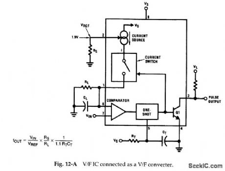
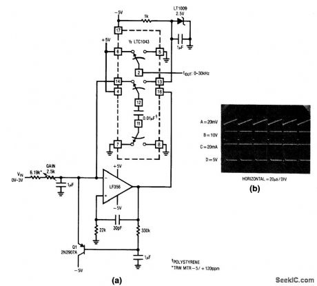
Fig. 12-2 In this circuit, the voltage input is applied to the noninverting input of the LF356, and the LTC1043 is connected in the LF356 feedback loop. This results in a V/F where the oscillation frequency is directly related to input voltage with a transfer linearity of 0.005%. To trim, apply 3.0 V, and adjust gain trim for a 30-kHz Output. Linear Technology, Linear Applications Handbook , 1990 p. AN3-11. (View)
View full Circuit Diagram | Comments | Reading(802)
| Pages:138/291 At 20121122123124125126127128129130131132133134135136137138139140Under 20 |
Circuit Categories
power supply circuit
Amplifier Circuit
Basic Circuit
LED and Light Circuit
Sensor Circuit
Signal Processing
Electrical Equipment Circuit
Control Circuit
Remote Control Circuit
A/D-D/A Converter Circuit
Audio Circuit
Measuring and Test Circuit
Communication Circuit
Computer-Related Circuit
555 Circuit
Automotive Circuit
Repairing Circuit