power supply circuit
High_side_MOSPET_driver
Published:2009/7/23 22:53:00 Author:Jessie | From:SeekIC

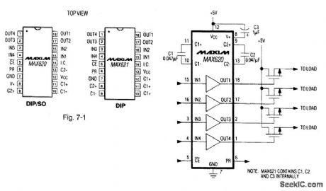
Figure 7-1 shows a MAX620 connected to power high-side switching and control circuits. The charge pump delivers a regulated output voltage that is 11 V higher than VCC to the drivers. In turn, the drivers translate a TTL/CMOS input signal to a noninverted output that swings from ground to the high-side voltage. The continuous driver-output current is 25 mA, with a typical quiescent current of 70 μA. The MAX620 requires three external charge-pump capacitors. The MAX621 has internal capacitors. MAXIM NEW RELEASES DATA Book, 1992, P. 4-19.
Reprinted Url Of This Article:
http://www.seekic.com/circuit_diagram/Power_Supply_Circuit/High_side_MOSPET_driver.html
Print this Page | Comments | Reading(3)

Article Categories
power supply circuit
Amplifier Circuit
Basic Circuit
LED and Light Circuit
Sensor Circuit
Signal Processing
Electrical Equipment Circuit
Control Circuit
Remote Control Circuit
A/D-D/A Converter Circuit
Audio Circuit
Measuring and Test Circuit
Communication Circuit
Computer-Related Circuit
555 Circuit
Automotive Circuit
Repairing Circuit
Code: