
Index 134
COMPARATOR_DETECTS_POWER_SUPPLY_OVERVOLTAGES,CATCHES_GLITCHES
Published:2009/7/7 3:59:00 Author:May
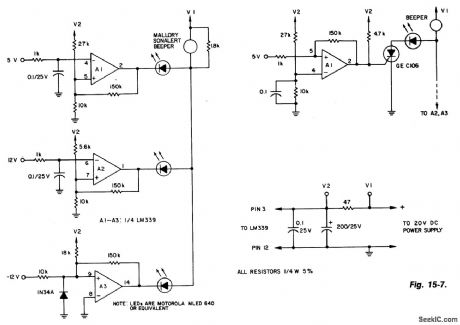
(A) To maintain an alarm condition when an overvoltage transient disappears, add an SCR to the comparator circuits. For SCR operation, voltages to the comparator inputs are inverted. (B) The triple-voltage monitoring circuit detects transient power-supply overvoltages. If excessive voltage momentarily appears at the 5, 12 and -12 V inputs, the LED for that circuit lights and the beeper sounds for as long as the overvoltage lasts. (View)
View full Circuit Diagram | Comments | Reading(1863)
Simple_ac_power_control
Published:2009/7/21 21:43:00 Author:Jessie

This circuit shows a simple ac full-wave control scheme that uses a triac and SBS. Control is obtained by varying the 100-kΩ pot. Notice that PGK can be omitted when triacs with nonsensitive gates are used. (View)
View full Circuit Diagram | Comments | Reading(823)
D_C_LEVEL_SHIFTER
Published:2009/7/21 22:22:00 Author:Jessie

Provides adjustable shift of up to 18 v in d-c voltage level of signal. -T. Mollinga, D-C Level Shifter Checks New Computer Modules, Electronics, 35:27, p 44-45.
(View)
View full Circuit Diagram | Comments | Reading(1)
OUBLE_SIDEBAND_SUPPRESSED_CARRIER
Published:2009/7/6 22:41:00 Author:May

Motorola MC1596G double-balanced modulator has carrier input between pins 8 and 7 and modulation between pins 1 and 4. Balancing carrier-null circuit, also connected between pins 1 and 4, contributes to excellent carrier rejection at output. For unbalanced output, ground one of push-pull output terminals. Requires two supplies.-E. M. Noll, Linear IC Principles, Experiments, and Projects, Howard W. Sams, Indianapolis, IN, 1974, p 138-139. (View)
View full Circuit Diagram | Comments | Reading(747)
Application circuit example of transistor switch stabilized voltage supply
Published:2011/4/23 4:16:00 Author:May | Keyword: transistor switch, stabilized voltage supply
The application of transistor switch stabilized voltage supply is rather widespread. The diagram is a specific circuit example.
In the diagram, transformer T, diode VD1~VD4 and capacitor C5 make up rectifying and wave-filtering circuit; sampling circuit is series by resistor R7, R8 and potentiometer R9;transistor Vr4 is error amplifier; switch adjuster is complex consisting of transistor Vr2, Vr3; Vt1 is pulse width adjuster; self oscillation circuit consists ofVT1, VT2, VT3 and R3, C3; reference voltage source consists of resistor R6 and constant voltage diode; VD5 is fly-wheel diode; L is energy storage induction; output filter consists of VD5, L and C12; the loop composed of R5 and C10 can make fly-wheel diode having better restitution property.
Bridge rectifier outputs DC voltage after breaking over AC network source switch S. Its positive end is connected with emitter of VT2 tube. Its negative end offers bias to Vr2 by resistor R2. It can make complex switch adjuster saturation and breaking over. Output current can generate induced voltage which the left is positive and the right is negative when it is passing energy storage induction L.
(View)
View full Circuit Diagram | Comments | Reading(850)
12_V_Battery_charger_control
Published:2009/7/22 3:27:00 Author:Jessie
This circuit shows the basic UJT building block (Fig. 9-1) that is used to control a battery-charger system. Notice that the battery voltage controls the charger and, when the battery is fully charged, the charger will not supply current to the battery. The setting of R2 determines the amount of charge. Also, the charger will not work if battery polarity is reversed. (View)
View full Circuit Diagram | Comments | Reading(1)
90_V_voltage_regulator_that_uses_a_PUT
Published:2009/7/22 4:17:00 Author:Jessie
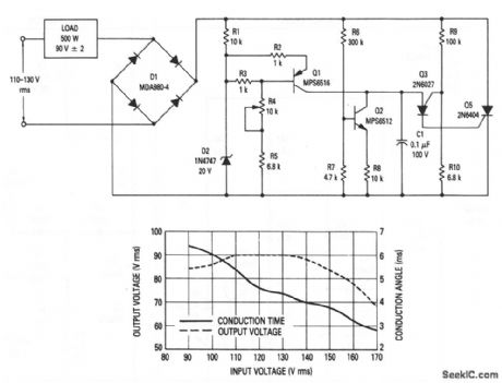
This circuit shows a PUT that is used to control a voltage regulator. Figure 9-28B shows a plot of output voltage and conduction angle versus input voltage for the regulator. The output voltage is set by R4. (View)
View full Circuit Diagram | Comments | Reading(670)
Battery_charger_that_uses_a_PUT
Published:2009/7/22 4:14:00 Author:Jessie
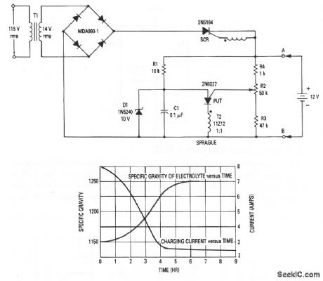
This circuit shows a PUT that is used to control a short-circuit-proof battery charger. Figure 9-27B shows the charging characteristics of the circuit. The charger provides an average charging current of about 8 A to a 12-V lead-acid storage battery. The circuit will not function or will be damaged by improperly connecting the battery because battery current is used to charge timing capacitor C1 (the SCR remains cut off, and the PUT relaxation oscillator does not function until a battery is connected as shown). The maximum battery voltage (10 to 14 V) is set by R2. (View)
View full Circuit Diagram | Comments | Reading(1711)
ELECTRIC_VEHICLE_BATTERY_SAVER
Published:2009/7/6 7:58:00 Author:May

The battery life and operating cost of an electric vehicle is severely affected by overdischarge of the battery .This circuit provides both warning and shutdown.An electronic switch is placed in senes with the propulsion motor contactor coil.Three modes of operation are possible:
· When the propulsion power pack voltageis above the 63-V tnp point,the electronic switch has no effect on operation
·When the propulsion power pack no load voltage IS below 63 V, power will not be supp⒒ed to the propulsion motor since the electronic switch will prevent contactor operation
· When the propulsion power pack loaded voltage drops below 63 V ,the contactor will close and open because of the electronic switch.The bucking operation indicates to the operator need to charge the batteries
(View)
View full Circuit Diagram | Comments | Reading(1074)
Program-controlled Power Supply Circuit of LM101
Published:2011/7/25 10:42:00 Author:Michel | Keyword: Program-controlled, Power Supply Circuit
The picture a and b are program-controlled power supply circuits.A1 and A2 in the circuit are followers work state and its input voltage are voltage drop on R6 or R12.The current flows through R6 or R10 is provided by 1 mA constant current of the constant current source.Picture (a) is +2~+38V positive output voltage and picture (b) is negative output voltage circuit.There is output short-circuit protection circuit in LM101.There is no large current when it is short circuit.C1 or C2 frequency compensates capacitance.The capacitive load is connected to output end and the circuit can work steadily. (View)
View full Circuit Diagram | Comments | Reading(518)
POWER_BOOSTER_2
Published:2009/7/6 7:07:00 Author:May
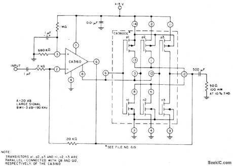
CA3600E CMOS transistor array provides parallel-connected transistors for power-boosting capability with CA3160 opamp. Feedback is used to establish closed. loop gain of 20 dB, Typical large-signal band-width (-3 dB) is 190 kHz, - Linear Integrated Circuits and MOS/FET 's, RCA Solid State Division, Somerville, NJ, 1977, p 271-273. (View)
View full Circuit Diagram | Comments | Reading(837)
METER_CALIBRATING_POWER_SUPPLY
Published:2009/7/22 23:45:00 Author:Jessie
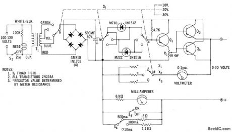
Provides adjustable regulated voltage up to 30 v. Zener diode regulation gives immunity to line voltage variations, giving performance equivalent to that of battery bias packs. Can also be used for testing transistors.- Zener Diode Handbook, International Rectifier Corp., 1960, p 61.
(View)
View full Circuit Diagram | Comments | Reading(1093)
LOW_VOLTAGE_POWER
Published:2009/7/6 5:29:00 Author:May
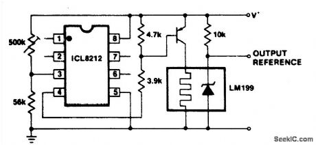
There are some classes of circuits that require the power supply to be disconnected if the power supply voltage falls below a certain value. As an example, the National LM199 precision reference has an on chip heater which malfunctions with supply voltages below 9 volts causing an excessive device temperature. The ICL8212 can be used to detect a power supply voltage of 9 volts and turn the power supply off to the LM199 heater section below that voltage. (View)
View full Circuit Diagram | Comments | Reading(762)
AUTOMATIC_SHUTOFF_FOR_BATTERY_POWERED_PROJECTS
Published:2009/7/6 5:21:00 Author:May
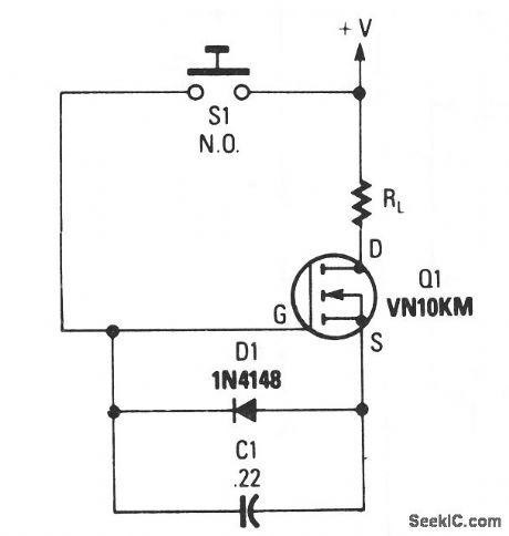
When S1 is depressed, C1 begins to charge to the supply voltage. That places a forward bias on the gate of Q1 turning it on and supplying current to load resistor RL. When the charge on C1 leaks off, the transistor shuts off, cutting off current to the load. That load could be anything from a transistor radio to a child's toy. Transistor Q1, available from Radio Shack as part No. 276-2070, is rated at 0.5 A at 60 Vdc. With a supply voltage of 9 Vdc and with C1 rated at 0.22 μF, a delay of about one minute is produced; with C1 rated at 10 μF, the delay is about an hour. (View)
View full Circuit Diagram | Comments | Reading(814)
Half-bridge switching regulated power supply circuit composed of CW1524
Published:2011/5/10 1:44:00 Author:Rebekka | Keyword: Half-bridge switching regulated power supply

Half-bridge switching regulated power supply circuit composed of CW1524 is shown as above. (View)
View full Circuit Diagram | Comments | Reading(1190)
UNIVERSAL_BATTERY_CHARGER_1
Published:2009/7/6 4:59:00 Author:May
The charger's output voltage is adjustable and regulated, and has an adjustable constant-current charging circuit that makes it easy to use with most NiCad batteries. The charger can charge a single cell or a number of series-connected cells up to a maximum of 18 V.
Power transistors Q1 and Q2 are connected as series regulators to control the battery charger's output voltage and charge-current rate. An LM317 adjustable voltage regulator supplies the drive signal to the bases of power transistors Q1 and Q2. Potentiometer R9 sets the output-voltage level. A current-sampling resistor, R8 (a 0.1- Ω, 5-W unit), is connected between the negative output lead and circuit ground. For each amp of charging that flows through R8, a 100 mV output is developed across it. The voltage developed across R8 is fed to one input of comparator U3. The other input of the comparator is connected to variable resistor R10.
As the charging voltage across the battery begins to drop, the current through R8 decreases. Then the voltage feeding pin 5 of U3 decreases, and the comparator output follows, turning Q3 back off, which completes the signal's circular path to regulate the battery's charging current.
The charging current can be set by adjusting R10 for the desired current. The circuit's output voltage is set by R9. (View)
View full Circuit Diagram | Comments | Reading(1992)
PORTABLE_NICAD_BATTERY_CHARGER
Published:2009/7/6 4:40:00 Author:May
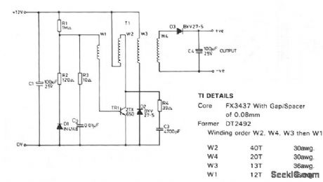
This circuit was designed to charge NiCad battery packs in the range of 4.8 to 15.6 V from a convenient remote power source, such as an automobile battery. When power is first applied to the circuit, a small bias current supplied by R1 via winding W1, starts to turn on the transistor TR1. This forces a volt-age across W2 and the positive feedback given by the coupling of W1 and W2 causes the transistor to turn hard on, applying the full supply across W2. The base drive voltage induced across W1 makes the junction between R1 and R2 become negative with respect to the 0-V supply, forward-biasing diode Dl to provide the necessary base current to hold TR1 on.
With the transistor on, a magnetizing current builds up in W2, which eventually saturates the ferrite core of transformer T1. This results in a sudden increase on the collector current flowing through TR1, causing its collector-emitter voltage to rise, and thus reducing the voltage across W2. The current flowing in W2 forces the collector voltage of the TR1 to swing positive until restricted by transformer output load-ing. Rc network R4 and C3 limits the turn off transient TR1. R3 and C2 maintain the loop gain of the circuit when diode D1 is not conducting.
(View)
View full Circuit Diagram | Comments | Reading(866)
Dc_stabilized_1000_V_μs_op_amp
Published:2009/7/23 20:10:00 Author:Jessie

As shown,this circuit has a full power bandwidth to 8 MHz,with a slewrate of 1000-V/μs. (View)
View full Circuit Diagram | Comments | Reading(853)
UJT_BATTERY_CHARGER
Published:2009/7/6 4:38:00 Author:May

This circuit will not work unless the battery to be charged is connected with proper polarity. The battery voltage controls the charger and when the battery is fully charged, the charger will not supply current to the battery. The battery charging the current is obtained through the SCR when it is triggered into the conducting state by the UJT relaxation oscillator. The oscillator is only activated when the battery voltage is low.VB21 of the UJT is derived from the voltage of the battery to be charged, and since VP=VD=VB21; the higher VB21,the higher Vp. When Vp exceeds the breakdown voltage of the zener diode Z1, the UJT will cease to ftre and the SCR will not conduct. This indicates that the battery has attained its desired charge as set by R2. (View)
View full Circuit Diagram | Comments | Reading(1832)
UNIVERSAL_BATTERY_CHARGER
Published:2009/7/6 4:34:00 Author:May

When power is applied to the circuit, SCR1 is off, so there is no bias-current path to ground; thus, LM317 acts as a current regulator. The LM317 is connected to the battery through steering diode D1, limiting resistor R1, and bias resistor R2. The steering diode prevents the battery from discharging through the LED and the SCR when power is removed from the circuit. As the battery charges, the voltage across trip-point potentiometer R5 rises, and at some point, turns on the SCR.Then, current from the regulator can flow to ground, so the regulator now functions in the voltage mode. When the SCR turns on, it also provides LED1 with a path to ground through R3. So, when LED1 is on, the circuit is in the voltage-regulating mode; when LED1 is off, the circuit is in the current-regulating mode. (View)
View full Circuit Diagram | Comments | Reading(5264)
| Pages:134/291 At 20121122123124125126127128129130131132133134135136137138139140Under 20 |
Circuit Categories
power supply circuit
Amplifier Circuit
Basic Circuit
LED and Light Circuit
Sensor Circuit
Signal Processing
Electrical Equipment Circuit
Control Circuit
Remote Control Circuit
A/D-D/A Converter Circuit
Audio Circuit
Measuring and Test Circuit
Communication Circuit
Computer-Related Circuit
555 Circuit
Automotive Circuit
Repairing Circuit