power supply circuit
PORTABLE_NICAD_BATTERY_CHARGER
Published:2009/7/6 4:40:00 Author:May | From:SeekIC

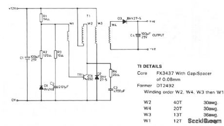
This circuit was designed to charge NiCad battery packs in the range of 4.8 to 15.6 V from a convenient remote power source, such as an automobile battery. When power is first applied to the circuit, a small bias current supplied by R1 via winding W1, starts to turn on the transistor TR1. This forces a volt-age across W2 and the positive feedback given by the coupling of W1 and W2 causes the transistor to turn hard on, applying the full supply across W2. The base drive voltage induced across W1 makes the junction between R1 and R2 become negative with respect to the 0-V supply, forward-biasing diode Dl to provide the necessary base current to hold TR1 on.
With the transistor on, a magnetizing current builds up in W2, which eventually saturates the ferrite core of transformer T1. This results in a sudden increase on the collector current flowing through TR1, causing its collector-emitter voltage to rise, and thus reducing the voltage across W2. The current flowing in W2 forces the collector voltage of the TR1 to swing positive until restricted by transformer output load-ing. Rc network R4 and C3 limits the turn off transient TR1. R3 and C2 maintain the loop gain of the circuit when diode D1 is not conducting.
Reprinted Url Of This Article:
http://www.seekic.com/circuit_diagram/Power_Supply_Circuit/PORTABLE_NICAD_BATTERY_CHARGER.html
Print this Page | Comments | Reading(3)

Article Categories
power supply circuit
Amplifier Circuit
Basic Circuit
LED and Light Circuit
Sensor Circuit
Signal Processing
Electrical Equipment Circuit
Control Circuit
Remote Control Circuit
A/D-D/A Converter Circuit
Audio Circuit
Measuring and Test Circuit
Communication Circuit
Computer-Related Circuit
555 Circuit
Automotive Circuit
Repairing Circuit
Code: