
Index 84
The AD693 power consumption reducing circuit with a parallel external power tube
Published:2012/8/26 22:40:00 Author:Ecco | Keyword: power consumption reducing , parallel , external power tube

In the AD693, output transistor VT1 has the maximum power consumption, if necessary, it can use external power tubes connected in parallel to reduce their power consumption, the circuit is shown in the figure. VT2 can select 2N1711 or 2N2219A NPN power tube, its base connects to OUT-end, the collecting electrode connects to BOOST ends. It requires power tube's cutoff frequency fT=10~100MHz, AC current amplification coefficient β >10. 2N1711 and 2N2219A's main parameter: UCEO=75V, ICM=0.8A,PCM=0. 8W.
(View)
View full Circuit Diagram | Comments | Reading(1244)
Typical application circuit of the integrated current sensor MAX472
Published:2012/8/26 22:29:00 Author:Ecco | Keyword: Typical application , integrated current sensor


UCC termination is connected to load or charger, or power supply and battery pack. RG1 and RG2 are external gain resistors. R1, ROUT are respectively pull-up resistor and output resistor. With MAX472, the external component values can be selected according to the following table.
(View)
View full Circuit Diagram | Comments | Reading(1433)
6 outputs circuit of integrated speed/voltage converter LM2907/2917
Published:2012/8/27 1:13:00 Author:Ecco | Keyword: 6 outputs , integrated , speed converter, voltage converter

(a)Overspeed alarm indication circuit
(b)Overspeed alarm indication circuit with hysteresis
(c)Ground load
(d)Voltage follower
(e)Voltage/current converter
(f)Integrating circuit
(View)
View full Circuit Diagram | Comments | Reading(1402)
The current loop interface of D/A converter (1B22 isolated programmable voltage/current sensor)
Published:2012/8/26 21:46:00 Author:Ecco | Keyword: current loop , interface , D/A converter , isolated , programmable, voltage sensor, current sensor

The circuit can convert the analog voltage generated by D/A converter to isolated 4~20mA output current. D/A converter can use AD7245 (12-bit DAC) model, and its output voltage range is set to 0~10V. Using 1B22 can achieve circuit isolation and output over voltage protection.
(View)
View full Circuit Diagram | Comments | Reading(1619)
The brightness adjustment circuit with gated switch ( visible brightness sensor LX1970 )
Published:2012/8/26 22:08:00 Author:Ecco | Keyword: brightness adjustment , gated switch , visible , brightness sensor

This circuit has the following characteristics: Firstly, it uses a CMOS gate circuit to control the power on-off of LX1970, only when the output of gate is high, LX1970 get electricity, LX1970 is a micro -power device, so the supply voltage can be provided by gate; Secondly, SRC end is connected to an isolation diode (VD ) in series, when LX1970 power down, VD is cut to play a role in isolation, the luminance signal can not be added to the LX1970; Thirdly, + 3.3V DC voltage signal and PWM signal can be equivalent to the two input signals of the logic oR gate, therefore, changing the DC voltage can also adjust the brightness. VD uses 1N4148 high-speed switching silicon diode.
(View)
View full Circuit Diagram | Comments | Reading(642)
Brightness adjustment circuit with visible brightness sensor LX1970
Published:2012/8/26 22:50:00 Author:Ecco | Keyword: Brightness adjustment , visible brightness sensor
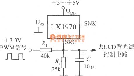
It only needs to change duty cycle of PWM (pulse width modulation) signal, the backlight brightness can be adjusted to suit individual needs. PWM signal voltage range is 3. 3V.
(View)
View full Circuit Diagram | Comments | Reading(539)
Burn-in circuit with aluminum electrolytic capacitor
Published:2012/8/24 21:36:00 Author:Ecco | Keyword: Burn-in circuit , aluminum electrolytic capacitor
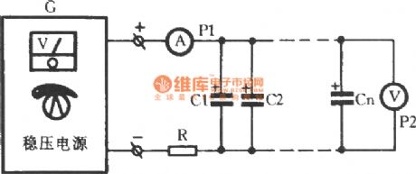
The burn-in of electrolytic capacitors is an effective way to reduce its leakage current. Burn-in method is shown as the figure. In the figure, G is a regulated power supply voltage, and its maximum current is above 1.5A. P1 is DC milliammeter with above 500mA range; P2 is DC voltmeter which is sectected according burn-in voltage value. The R -limiting resistor: resistance is selected by burn-in capacitor rated working voltage with 1V taking 1Ω. If the burn-in capacitor rated voltage is greater than 100V, R take, 1kΩ, the power of resistor R should be greater than 2W, depending on the value of parallel capacitor.
(View)
View full Circuit Diagram | Comments | Reading(1524)
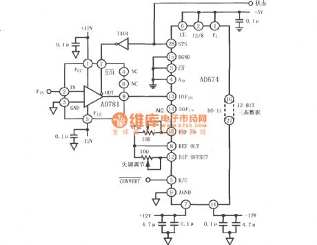
Interface circuit of sample and hold amplifiers AD781 and AD674
Published:2012/8/24 21:48:00 Author:Ecco | Keyword: Interface circuit , sample and hold , amplifier
View full Circuit Diagram | Comments | Reading(1039)
The basic connection circuit of sample and hold amplifier AD9101
Published:2012/8/24 22:00:00 Author:Ecco | Keyword: basic connection , sample and hold , amplifier
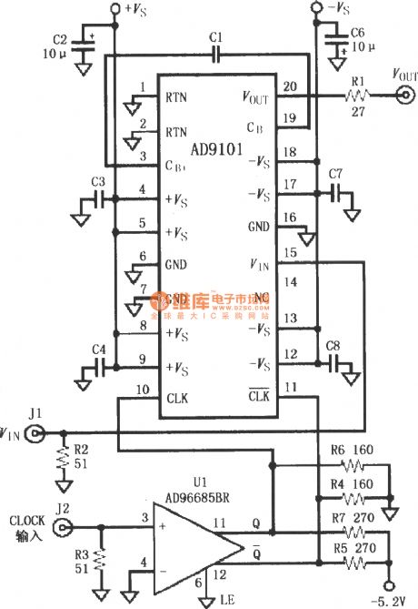
AD9101 is built-in the holding capacitor CHOLD, and sample-and-hold is controlled by the CLOCK. According to basic connection diagram, RTN grounds to keep the gain of the amplifier in 4. The noninverting input terminal of ultrafast comparator AD96685BR produced by the Analog Devices Inc. is added the clock input, then Q is sent to AD9100's non CLK and CLK (10,11 feet) as the sampling and holding control signal. The capacitors without marking use 0.01μF; the selection of R1 should be subject to the load capacitor with considering the condition that load capacitance may be less than 6pF in short circuit.
(View)
View full Circuit Diagram | Comments | Reading(1289)
Two-channel switch circuit with sample-and-hold amplifier LF398
Published:2012/8/24 22:17:00 Author:Ecco | Keyword: Two -channel, switch , sample-and-hold, amplifier
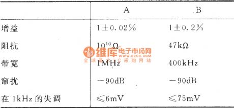
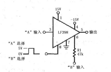
Two input signals A, B are respectively added to the input end ( pin 3 ) and sampling capacitor end ( pin 6 ), pin 8 is connected to selecting pulse, and the internal switch can be used to change channels A and B, when a pulse is high (5V ), the internal switch is closed, the output is the A channel signal; when the selection pulse is low (0V), the internal switch is turned off, the signal output is the B channel. The parameters of the channel A, B are shown in the table below.
(View)
View full Circuit Diagram | Comments | Reading(3311)
The GPS receiver downconverter circuit with MAX2682
Published:2012/8/25 1:29:00 Author:Ecco | Keyword: GPS receiver , downconverter
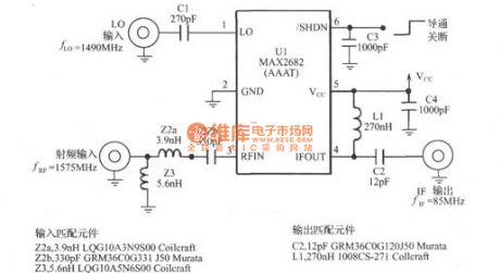
The typical application circuit of MAX2680/MAX2681/MAX2682 is shown as following:
(View)
View full Circuit Diagram | Comments | Reading(1011)
RF2498-based GPS receiver downconverter circuit
Published:2012/8/25 1:53:00 Author:Ecco | Keyword: GPS receiver , downconverter

RF2498 is a high-performance CDMA band / dual mode integrated LNA / mixer circuit, a three- band LNA / downconverter. RF2498 can be used in CDMA / Cellular / PCS / GPS handheld devices, JCDMA / GSP handheld devices, CDMA modems / data cards, commercial and consumer systems, portable batteries. RF2498 meets the requirements of IS-98 sensitivity, interact modulation and tone adjustment. RF2498's gain control is 29dB in the PCS band and gain control 27.5dB in cellular band. RF2498 provides 37dB gain for a GPS LNA / mixer application. The RF2498 uses three-state gain control mode to meet the IS-98 IMD test. The chip has an integrated TX LO buffer.
(View)
View full Circuit Diagram | Comments | Reading(1909)
μPB1009K - based GPS receiver RF front-end circuit
Published:2012/8/25 1:28:00 Author:Ecco | Keyword: GPS receiver , RF front-end
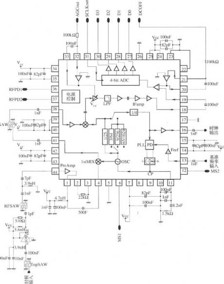
μPBl009K is a single-chip GPS receiver chip which integrates full VCO, the second stage IF ( intermediate frequency ) filter, 4bit ADC, digital control interface circuit.μPBl009K has the double conversion function: fREFin = 16.368 MHz f1stFin = 61.380MHz f2dFin = 4.092 MHz ; fREFin 14.4/16.384/19.2/26MHz f1stFin = 62.980MHz f2ndIFin = 2 . 556MHz. It has a multi - system clock. With frequency divider ( 1 / N = 100,3 / 256,9 / 1024,65 / 4096 ) on the conversion sheet, TCXO frequency can be 16.368MHz/16.384MHz, 14.4MHz, 19 .2 MHz, or 26MHz. The power supply voltage Vcc = 2.7V - 3.3V. Low current consumption : lcc = 26.0mA.μPBl009K can be applied to the GPS receiver with reference frequency in 16.368MHz, the second-stage IF frequency in 4.092MHz, and the GPS receiver with reference frequency in 14.4MHz , 16.384MHz, 19.2MHz and 26MHz, the second-stage IF frequency in 2.556MHz.
(View)
View full Circuit Diagram | Comments | Reading(2355)
GP2015 - based GPS receiver RF front-end circuit
Published:2012/8/25 1:10:00 Author:Ecco | Keyword: GPS receiver, RF, front-end


The GP2015 is a GPS receiver RF front-end circuit which provides a low- power, low-cost and high reliability GPs RF front-end solution. With the same performance of GP2010, GP2015 uses TQFP-48 package, 3V to 5V operating supply voltage, 200mW (3V voltage) power consumption. Ll (1575.42MHz) C / A (Coarse-Acquisition) code signal is input to GP2015 by the antenna and low noise amplifier to output is a 2bit digital signal. The GP2015 includes an on-chip synthesizer, mixer, automatic gain control (AGC), and a quantizer which can provide sign and magnitude digital output. A complete GPS receiver RF front-end circuit only requires minimal external components.
(View)
View full Circuit Diagram | Comments | Reading(2197)
GPl020-based 6-channel correlator circuit
Published:2012/8/25 1:21:00 Author:Ecco | Keyword: 6-channel correlator
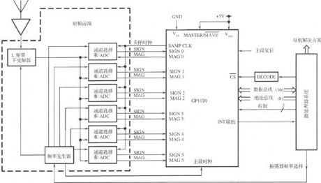
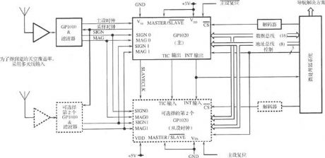
GPl020 is a 6-channel CMOS digital correlator which can be used with GPl010 L1 channel down converter or other integrated circuit to intercept and track the GPS C / A code or GLONASS code. Each channel of 6 channels in GPl020 includes: separate digital downconverted to baseband processing circuit, C / A code generator, correlator and accumulation dump register. GPl020 connects to the interface of a microprocessor by a 16-bit data bus, and it uses different on-chip registers to control the process of acquisition and tracking. The input multiplexer is suitable for GPS front end and GLONASS front end, allowing antenna differences. Supply voltage of the circuit is 5v, power consumption is less than 500mW, and it is available in 120L MQFP package with size in 28mm × 28mm × 3.4mm.
(View)
View full Circuit Diagram | Comments | Reading(1275)
MAX2641-based GPS receiver LNA circuit
Published:2012/8/25 1:14:00 Author:Ecco | Keyword: GPS receiver, LNA
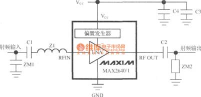
The MAX2641 is alow-price, ultra - low noise LNA whichcan be used in cellular phones, PCS, GPS, and 2.4GHz ISM band.With single-ended power supply, thevoltage is +2.7 V to +5.5 V , the current consumption is 3.5mA.
MAX2641's frequency rangeis 1400MHz ~ 2500MHz, typical gainis 15.7dB, the input IP3is 4dBm, noise figureis 1.2dB at 1575MHz. MAX2641 usesinternal bias circuit without external bias resistors and chokes. It requires the input matching network withonly two components,input / output blocking capacitor and VCC bypass capacitor. It is available in SOT23-6 package.
(View)
View full Circuit Diagram | Comments | Reading(1580)
MRFICl505R2 - based GPS receiver RF front-end circuit
Published:2012/8/25 0:56:00 Author:Ecco | Keyword: GPS receiver , RF, front-end

MRFICl505R2 is a 1.575GHz GPS downconverter chip. It integrates mixer, VCO, PLL, crystal oscillator, A / D converter and loop filter and other circuits. MRFICl505R2 IF output frequency is 4.1MHz; it has 105dB typical conversion gain, 2.7V operating voltage, 28mA typical current consumption; it is available in LQFP-48 package.
(View)
View full Circuit Diagram | Comments | Reading(1685)
Two regulators connecting in series to get 0 ~ 284V voltage
Published:2012/8/23 22:46:00 Author:Ecco | Keyword: Two regulators, connecting, in series, 0 ~ 284V voltage
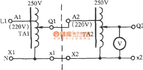
As shown in the figure, the two regulators TAl and TA2 are connected in series to obtain 0 ~ 284V voltage. The two regulators' X1, X2 are connected with a wire together, then the power zero line N is connected;220V power supply is connected between Al andX1. The output terminal Q1 of TA1 is connected to A2 end of TA2. After energized,it can get 0 ~ 284V voltage betweenTA2 outputend andQ2, and voltage regulator issmooth.
(View)
View full Circuit Diagram | Comments | Reading(627)
Three regulators with star connection to get 0 ~ 433V voltage
Published:2012/8/23 22:40:00 Author:Ecco | Keyword: Three regulators , star connection , 0 ~ 433V voltage
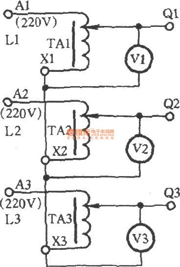
As shown in the figure, three regulators TA1 , TA2, TA3 are connectedas star connection to expand pressure range and get the maximum attainable 433V voltage . The three regulators' X1, X2, X3 ends areconnected together, A1 , A2 , A3 are respectively connected to the 380V power's L1, L2, L3 three phases, so itobtains 433V at the output terminals Q1 and Q2 or Q2 or Q3 ends. This connection requires a three-phase voltage balance, TA1, TA2 and TA3 models and specifications must be the same.
(View)
View full Circuit Diagram | Comments | Reading(737)
The analog USB with homemade USB port ISP2313
Published:2012/8/23 22:54:00 Author:Ecco | Keyword: analog USB , homemade, USB port


Many laptops have no serial or parallel port. In this case, people only can use the USB port ISP. The production is not using a real USB chip, but with 2313 to copy USB timing.
(View)
View full Circuit Diagram | Comments | Reading(1067)
| Pages:84/471 At 2081828384858687888990919293949596979899100Under 20 |
Circuit Categories
power supply circuit
Amplifier Circuit
Basic Circuit
LED and Light Circuit
Sensor Circuit
Signal Processing
Electrical Equipment Circuit
Control Circuit
Remote Control Circuit
A/D-D/A Converter Circuit
Audio Circuit
Measuring and Test Circuit
Communication Circuit
Computer-Related Circuit
555 Circuit
Automotive Circuit
Repairing Circuit