
Index 88
The bias zeroing circuit of logarithm and logarithmic ratio amplifier LOG100
Published:2012/8/13 21:43:00 Author:Ecco | Keyword: bias , zeroing circuit , logarithm, logarithmic, ratio amplifier

The circuit uses two 10kΩ potentiometers R2 , R2 to make zero set for input bias current ofinternal amplifiers A1, A2. Internal amplifiers A1 , A2are field effect transistor (FET) inputs, so the FET inputs havebias current feature which meansthe temperature increases 10 ℃, input bias current will be doubling. This bias zeroingcircuit can beonly used for the occasions with stable temperature.
(View)
View full Circuit Diagram | Comments | Reading(1011)
The current reverse input circuit of logarithm and logarithmic ratio amplifier LOG100
Published:2012/8/13 21:36:00 Author:Ecco | Keyword: current , reverse input , logarithm , logarithmic, ratio amplifier

LOG100's input current is positive current, andit means usually the input current can only flow to pin 1 and pin 14. In some applications, the signal current is negative current , such as photomultiplier tubes. The circuit can solve this problem, which uses the circuit in the attached diagramto convertnegative signal current to positivecurrent inflowing toLOG100.
(View)
View full Circuit Diagram | Comments | Reading(929)
General application circuit diagram of three-terminal adjustable output regulator
Published:2012/8/12 21:08:00 Author:Ecco | Keyword: General application , three-terminal , adjustable output , regulator

Figure 1 shows the general application circuitof three-terminal adjustable positive output integrated voltage regulator circuit ( adjustable negative output voltage regulator has a similar circuit). In the circuit, R1 and RP form the resistor network with adjustable output. in order to makebias current and the tube's leakage currentbe absorbed, R1 is set in the range of 120 ~ 240Ω .The discharge currentflowing throughR1 is 5 ~ 10mA. The input capacitor C1 is used to suppress the ripple voltage. The output capacitor C is used to eliminate vibration andbuffer the impact of load to guarantee the stability of the circuit operation.
(View)
View full Circuit Diagram | Comments | Reading(835)
The capacitive lag compensation circuit composed of LF398
Published:2012/8/13 22:15:00 Author:Ecco | Keyword: capacitive lag compensation

C1, R1 , R2 andR3 constitute a capacitance lag compensation circuit,and the time constant C1 = τ/100kΩ; adjusting potentiometer R3 can adjust the output amplitude.
(View)
View full Circuit Diagram | Comments | Reading(1465)
The basic circuit diagram of mirror constant current source
Published:2012/8/12 20:52:00 Author:Ecco | Keyword: basic circuit , mirror , constant current source


The basic circuit of the mirror constant current source is shown as the figure,and VT1, VT2 are MAPs. From the figure, the Ir = Ic2 + IB1 + IB2. Because VT1, VT2are symmetrical, the collector currentis equal tobase current, so
When Ir is determined, the constant current source output current Io is also identified. When β is large enough , Io ≈ Ir, and that is, the output current is approximately equal to the reference current , the circuit is often referred to a current mirror circuit.
(View)
View full Circuit Diagram | Comments | Reading(1454)
Grating circuits using integrated circuit
Published:2012/8/14 3:16:00 Author:Ecco | Keyword: Grating circuits, integrated circuit

This circuit uses TAA293 as a threshold switch. 1KΩ resistor is used to adjust the value of the photoresistor and threshold of threshold switch. Two circuits are suitable for the occasions: the light intensity is greater than 1000lx ( Q end is in high level) , light intensity is less than 300lx ( Q end is in low level).
(View)
View full Circuit Diagram | Comments | Reading(638)
TA7240AP internal block diagram and its main parameters
Published:2012/8/11 1:51:00 Author:Ecco | Keyword: internal block , parameters


TA7240AP is thestereo audio power amplifier IC produced by Japan's Toshiba Corp. It has high-fidelity, low-noise , high-power characteristics.It iswidely used in early audio equipments.
Its main parameters can be seen at the following table:
(View)
View full Circuit Diagram | Comments | Reading(1016)
Resistor - transistor gate circuit
Published:2012/8/11 1:48:00 Author:Ecco | Keyword: Resistor - transistor gate

Figure (a) is theresistor - transistor gate circuit diagram , it is similar to the ordinary NAND gate, but each input endisconnectedto a Rk with the samevalue.
Figure (b) shows its logic symbol .
(View)
View full Circuit Diagram | Comments | Reading(958)
Comparator circuit with hysteresis characteristics (Schmitt trigger )
Published:2012/8/11 1:39:00 Author:Ecco | Keyword: Comparator , hysteresis characteristics , Schmitt trigger
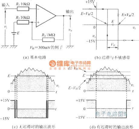
(a)The basic circuit; (b)Hysteresis and non- sensitive zone; (c)The output wave without hysteresis; (d)The output wave with hysteresis
(View)
View full Circuit Diagram | Comments | Reading(1673)
The level shift circuit diagram completed by PNP transistors
Published:2012/8/12 21:40:00 Author:Ecco | Keyword: level shift, PNP transistor

PNP transistor forms common-emitter amplifier circuit to ensure that the transistors work in the enlarged area, and the collector level must be less than the base level. So, in the NPN multi-stage DC amplifier circuit, inserting a PNP transistor common-emitter amplifier circuit can complete the displacement of DC level and zoom function. (View)
View full Circuit Diagram | Comments | Reading(5228)
The level shift circuit diagram completed by constant flow source
Published:2012/8/12 21:54:00 Author:Ecco | Keyword: level shift , constant flow source
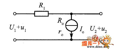
The DC internal resistor Ro of constant current source is very small, AC internal resistor ro is great, when the R1 》 Ro and R1 《 ro, the DC level U2 of output end is much lower than DC level U1 of the input end, namely U2 《 U1. AC voltage u2 of output end decreases little from input AC voltage u1, that is, u2 ≈ u1. Therefore, the circuit decreases DC level under the circumstance without losing AC voltage.
(View)
View full Circuit Diagram | Comments | Reading(699)
Practical circuit diagram to expand current with external PNP power transistor
Published:2012/8/12 21:59:00 Author:Ecco | Keyword: Practical circuit , expand current, external , PNP , power transistor
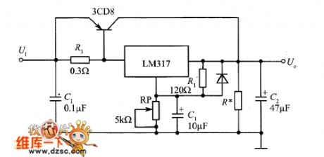
Expanding output current can be realized in two ways: connecting external high-power tubes; connected two or more integrated voltage regulators in parallel. The figure shows practical circuit using an external PNP power transistor to expand the output current, and the method is simple but reduces the precision of the regulator.
(View)
View full Circuit Diagram | Comments | Reading(1482)
The fixed low - voltage output circuit diagram of three-terminal adjustable output regulator
Published:2012/8/12 21:16:00 Author:Ecco | Keyword: fixed, low - voltage output , three-terminal , adjustable output, regulator
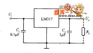
The figure shows the resistor network without adjustable outpu , and it gets 1.25V fixed low-voltage output circuit. The temperature drift is low, which is only decided by the temperature drift of internal reference voltage source.
(View)
View full Circuit Diagram | Comments | Reading(600)
Three-controller light switch circuit
Published:2012/8/1 2:30:00 Author:Ecco | Keyword: Three-controller, light switch

Three-controller switchmeans the circuit can independently control the same lamp's lighting or extinguishing in three different places, and the circuit is shown as the figure. In the figure S1 , S3, 1 × 2 are single - pole double-throw switches, and S2 uses the 2 × 2 DPDT switch.
(View)
View full Circuit Diagram | Comments | Reading(1988)
Typical application circuit of nRF401 single - chip RF transceiver
Published:2012/7/25 3:10:00 Author:Ecco | Keyword: Typical application, single - chip, RF transceiver


The nRF401 typical application circuit is shown as the figure. The UDD uses a +3 V power supply. The crystal oscillator circuit is composed of R1 , JT , C1 and C2; C3 , C4 and R2 form the loop filter. R3 can be used to set resistance for the power. C5 is the power decoupling capacitor, C6 and C7 are noise canceling capacitors. DIN and DOUT side are respectively connected the MCU's TXD port ( serial output ) , RXD port( serial input ). In order to simplify the circuit, nRF401 can connect with μC to be used as a crystal oscillator circuit, and it is shown as below. X1 and X2 are μC's crystal input and output ports, and the generating crystal frequency is sent directly to the XC2 side of nRF401.
(View)
View full Circuit Diagram | Comments | Reading(1228)
The converter IC circuit diagram
Published:2012/7/25 3:25:00 Author:Ecco | Keyword: converter IC


TDA8444is the D / A ( digital / analog ) converter IC produced by Philips, and it is used to convert digital signals to analog signals.1. pin functions and dataTDA8444 IC uses 16-pin double-row package, andpin functions and data are shown in Table 1 .
2. Typical application circuitTDA8444 and LM1036Nare matched byCPU to control the tone, volume , two-channel electronic balance. The the typical application circuit isshown in Figure 1.
(View)
View full Circuit Diagram | Comments | Reading(1887)
TDA8755 D/A converter IC circuit diagram
Published:2012/7/25 3:21:00 Author:Ecco | Keyword: D/A converter , IC


TDA8755 is the D / A ( digital / analog ) converter IC produced by philips company. It is suitable for A / D converter occasions such as the all applications included TV ( rear projection , LCD ), DVD players, instrumentation and so on.
(1) Functions and Features
TDA8755 integrated circuit includes a digital multi-channel converter, analog circuit converter, ADC circuit, digital encoder, clamping logic circuit, ADC interface circuit, tracking and maintaining circuit, timing generator, comparator circuit, power supply and regulator circuit and other auxiliary functions circuit. Its block diagram is shown in Figure 1.
(2) pin functions and dataThe TDA8755 IC uses 32-pin double-row hundred plug-in package,and pin functions and data are shown in Table 1 . (View)
View full Circuit Diagram | Comments | Reading(1687)
MAX264 filter circuit diagram
Published:2012/7/23 3:01:00 Author:Ecco | Keyword: filter

The system design uses a pin programmable filter MAX264 to realize low-pass or high pass filter, and the circuit is shown in the figure ( Attenuation amplification network). The circuit design uses unipolar input mode, and its input voltage range is 0 V to 5 V. When people adjust circuit, the signal should be adjusted to the input range. Conditioning process: the signal first passes the attenuation network to make the peak - the peak be -2.5 V ~ +2.5 V, then the adder adjusts the signal to the range of 0 V ~~ 5 V, after filtering , the subtractor turns signal into - 2.5 V ~ +2.5 V, and zoom network is used to compensate balance attenuation, then the circuit outputs the rms to converter circuit.
(View)
View full Circuit Diagram | Comments | Reading(1175)
LED AC driver circuit
Published:2012/7/18 3:08:00 Author:Ecco | Keyword: LED, AC driver
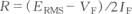
As shown in the figure, the circuit can work normally under the cases of unknown polarity of the voltage or power supply polaritybeing reversed or not. Being same with DC driver, the current limiting resistor values of R can de decided by the following formula when it is used as AC driver:
In the formula, ERMS is the effective value of AC voltage.
(View)
View full Circuit Diagram | Comments | Reading(1551)
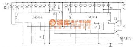
The bargraph display driver circuit with 20 light - emitting segments
Published:2012/7/18 3:25:00 Author:Ecco | Keyword: Bargraph display , driver , 20 , light - emitting segments
View full Circuit Diagram | Comments | Reading(1205)
| Pages:88/471 At 2081828384858687888990919293949596979899100Under 20 |
Circuit Categories
power supply circuit
Amplifier Circuit
Basic Circuit
LED and Light Circuit
Sensor Circuit
Signal Processing
Electrical Equipment Circuit
Control Circuit
Remote Control Circuit
A/D-D/A Converter Circuit
Audio Circuit
Measuring and Test Circuit
Communication Circuit
Computer-Related Circuit
555 Circuit
Automotive Circuit
Repairing Circuit