
Index 85
The interface circuit of sampling and maintaining amplifier AD9101
Published:2012/8/23 22:11:00 Author:Ecco | Keyword: interface circuit , sampling, maintaining, amplifier

When the signal frequency increases, the traditional fast sampling circuit is forced to sacrifice dynamic range for the stability of the overall performance. The circuit shown in figure uses AD9101 to match with high - speed 8 - bit A / D converter AD9002, the purpose is to enhance the high frequency performance of the Flash ADC; simultaneously with the regulator and output of op-amp voltage follower, the circuit increases AD9101 RTN feet potential to 0 .33 V.
(View)
View full Circuit Diagram | Comments | Reading(552)
The AD585 HOLD effective sample - hold circuit with gain = +2
Published:2012/8/23 22:16:00 Author:Ecco | Keyword: HOLD, effective , sample - hold , gain = +2
View full Circuit Diagram | Comments | Reading(1224)
Tracking - hold intermediate frequency (IF) signal acquisition circuit (AD9100/AD9618)
Published:2012/8/23 22:21:00 Author:Ecco | Keyword: Tracking - hold , intermediate frequency , signal acquisition
AD9100 has a wide dynamic range, and therefore can be used to capture the super signal, and it can directly convert the intermediate frequency signal (IF) to digital signal. After IF signal is input AD9100, T / H clock control sampling and holding, then the signal is output and amplified by AD9618, and the ADC circuit converts the analog signal to a digital signal. With reducing analog signal input level, the method can realize the track and hold with a minimum distortion; while adjusting the AD9618 gain, the analog signal range input to ADC meets the full scale range of the A / D converter - digital conversion.
(View)
View full Circuit Diagram | Comments | Reading(580)
Precision current inverter / current source circuit 1 composed of LOG101/104 and op amp OPA2335
Published:2012/8/23 21:36:00 Author:Ecco | Keyword: Precision , current inverter, current source , op amp
LOG101/104 's input current can only be positive current, that is, input current only flows into pin 1 and pin 8, which can be fine tuned as 10nA to 1mA. In some applications, the signal current is a negative current, such as: photomultiplier, tube, photodiode. The circuit shown in diagram can resolve this problem, which utilizes the circuit switch the negative signal current generated by photodiodes to a forward current flowing into LOG101.
(View)
View full Circuit Diagram | Comments | Reading(1375)
Precision current inverter / current source circuit 2 composed of LOG101/104 and op amp OPA2335
Published:2012/8/23 21:39:00 Author:Ecco | Keyword: Precision, current inverter , current source circuit , op amp
The negative signal current generated by the photodiodecan be converted to the forward current flowing into LOG101 by two op amps OPA2335.
(View)
View full Circuit Diagram | Comments | Reading(889)
Current allocation multiplexing circuit composed of double broadband transconductance operational amplifier OPA2662
Published:2012/8/23 21:57:00 Author:Ecco | Keyword: Current allocation , multiplexing, double broadband , transconductance, operational amplifier
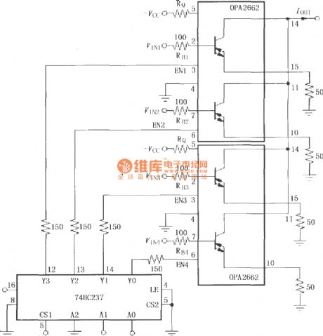
74HC237 is the address latch 3 line - to - 8 line decoder, three-way encoded signals A1, A2, A3 are input 74HC237 to decode and output decoded signals Y0 , Y1 , Y2, and Y3, and they can respectively control two OPA2662 and enable terminal EN to output different paths of current, then the current allocation multiplexing circuit is made up.
(View)
View full Circuit Diagram | Comments | Reading(1054)
Two-channel current output driver circuit composed of double broadband transconductance operational amplifier OPA2662
Published:2012/8/23 22:05:00 Author:Ecco | Keyword: Two-channel , current output , driver circuit , double broadband , transconductance, operational amplifier
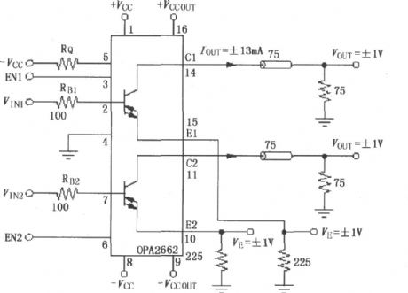
The circuit uses OPA2662 internal dual OTA to constitute two-channel current output driver circuit, and input signals VIN1 and VIN2 are amplified by OPA2662 to output current IOUT1 and IOUT2 for driving current to drive 75Ω cable and load. EN1, EN2 can control turning on or off of channels, when EN is in high level, the channel is turned on; when EN is in low level, the channel is turned off.
(View)
View full Circuit Diagram | Comments | Reading(1005)
The basic signal and power connection circuit of broadband transconductance operational amplifier and buffer OPA660
Published:2012/8/22 21:38:00 Author:Ecco | Keyword: basic , signal , power, connection , broadband , transconductance, operational amplifier , buffer

It is the connection circuit for op amp OPA660, the signal is input by pin 3, then pin 8 will output current after the signal being amplified. Power supply terminal uses bypass capacitor filter which preferably uses solid tantalum capacitor as a filter capacitor, and the design of the PCB should allow the filter capacitor to close to the power supply terminal. Quiescent current is set by external resistor RQ connected to pin 1 and -VCc, and the change of resistor RQ can affect internal OTA of OPA660 to control their bandwidth, AC performance and transconductance. When ambient temperature at 25 ℃, OPA660 provides typically 20mA total quiescent current IQ, and that can be eached by setting RQ = 250Ω. The quiescent current IQ can change in the range of 16 ~ 26mA when RQ is fixed as 250Ω.
(View)
View full Circuit Diagram | Comments | Reading(1232)
The antilogarithm circuit composed of logarithmic and logarithmic ratio amplifier LOG100
Published:2012/8/22 21:47:00 Author:Ecco | Keyword: antilogarithm , logarithmic , logarithmic ratio , amplifier
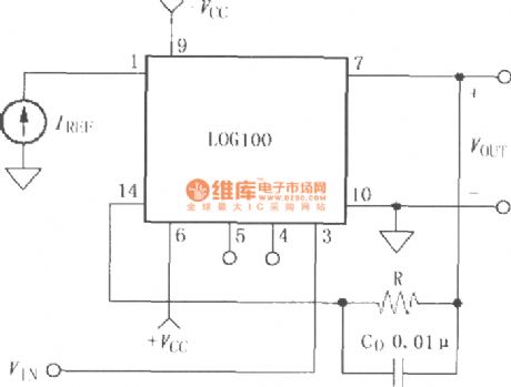
The circuit transformslogarithmic amplifier LOG100into antilog circuit. When VIN connects to pin 3, k=1; when VIN connects to pin 4, K =3; when VIN connects to pin 5, K =5.
(View)
View full Circuit Diagram | Comments | Reading(671)
Video luminance matrix circuit composed of broadband transconductance op amp and buffer OPA660
Published:2012/8/22 21:59:00 Author:Ecco | Keyword: Video, luminance matrix , broadband transconductance, op amp , buffer
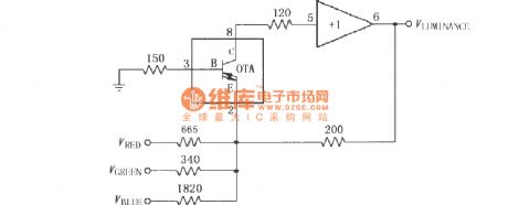
The OPA660 forms a common-base amplifier circuit, and its pin 2 has three-way signal inputs: red VRED, green VGREEN and blue VBLUE, the signals are amplified by internal OTA and +1 amplifier to become luminance signal VLUMINANCE which is output from pin 6. The accuracy of the resistor connected to three-way signals is 1 %, resulting in the RGB mixing ratio of 30%: 59%: 11%.
(View)
View full Circuit Diagram | Comments | Reading(1219)
Voltage buffer circuit with twice of output current composed of broadband transconductance op amp and buffer OPA660
Published:2012/8/22 22:18:00 Author:Ecco | Keyword: Voltage buffer , twice , output current, broadband transconductance , op amp , buffer


The essence of this circuit common collector ( total -C) amplifier circuit of OPA660, and it uses a common collector (Total -C) amplifier circuit's current amplification effects to set the resistor of OTA in figure and current gain in 2, then to form a voltage buffer with twice of output current. Parameter settings are shown in the table below.
(View)
View full Circuit Diagram | Comments | Reading(860)
Logarithmic function-transformation circuit with negative input current I1 ( logarithmic amplifier 4127)
Published:2012/8/22 21:42:00 Author:Ecco | Keyword: Logarithmic, function-transformation circuit, negative input current, I1 , logarithmic amplifier

As shown in the figure, the circuit is logarithmic function-transformation circuit when thesignal I1is input asvoltage form and I1 is a negative. When the input I1 is added to pin 7 of 4127 with negative direction, the output voltage Eo=-A•log(|I1|/ IR), then output is transformed to logarithmic form.
(View)
View full Circuit Diagram | Comments | Reading(652)
Single-end input, double-end output differential line driver circuit composed of OPA2662
Published:2012/8/22 22:24:00 Author:Ecco | Keyword: Single-end input, double-end output, differential, line driver

It usestwo identical amplifiers contained in dual op amp OPA2662 to form the circuit shown in Figure, OTA2's inputend -pin 7 is grounded by 100 resistor, OTA1 input end -pin 2 is the input end,and the single-end input signal VIN is amplified by pin 14 and and output pin 11.
(View)
View full Circuit Diagram | Comments | Reading(1692)
1600 × 1200 high-resolution graphics monitor CRT output stage driver circuit composed of OPA2662
Published:2012/8/22 22:28:00 Author:Ecco | Keyword: 1600 × 1200 , high-resolution , graphics monitor, CRT, output stage, driver

The circuit utilizes OPA2662's internal two OTAs to constitute a common-emitter amplifier, that is, input end is added 150Ω current limiting resistor and 50Ω termination resistor, and the signal is amplifed to pass CR3425 and drive CRT monitor. At the input end, , tR = 0.7 ns , tF = 0.7 ns ; , tR = 2.4ns , tF = 2.15ns.
(View)
View full Circuit Diagram | Comments | Reading(821)
Logarithmic function-transformation circuit with negative input voltage E1 ( logarithmic amplifier 4127)
Published:2012/8/22 21:22:00 Author:Ecco | Keyword: Logarithmic, function-transformation circuit , negative input voltage, E1, logarithmic amplifier

As shown in the figure, the circuit is logarithmic function-transformation circuit when thesignal E1is input asvoltage form and E1 is a negative. When the input E1 is added to pin 7 of 4127 with negative direction, the output voltage Eo=-A•log(|E1|/R4 • IR), then output is transformed to logarithmic form.
(View)
View full Circuit Diagram | Comments | Reading(1431)
Drift zeroing circuit of logarithmic and logarithmic ratio amplifier LOG101/104
Published:2012/8/22 21:02:00 Author:Ecco | Keyword: Drift zeroing , logarithmic , logarithmic ratio , amplifier

LOG101/104 input current I1/I2 is limited in the range of 100pA ~ 3.5mA, and if input current is greater than 3.5mA, the nonlinearly will be increased; if input current is less than 100pA, the input bias current ( typical value 5pA) will cause the input error to increase. When ± 5V supply operates, the input current (I1 + I2) is limited to 4.5mA. The circuit uses two 10kΩ potentiometers R2, R'2 to zero the input bias current of internal amplifiers A1 , A2. The internal amplifiers A1 , A2 control the field - effect transistor (FET) input, so the FET input has bias current characteristics, and temperature increases to 10 ℃ will double the input bias current.
(View)
View full Circuit Diagram | Comments | Reading(674)
Basic signal and power connection circuit of logarithmic and logarithmic ratio amplifier LOG101/104
Published:2012/8/22 21:11:00 Author:Ecco | Keyword: Basic, signal , power, connection , logarithmic, logarithmic ratio , amplifier

Signal current I1/I2 is input to pin 1 and pin 8, then pin 3 outputs voltage VOUT = (1V) · log (I1/I2). In order to reduce the impact of the wire inductance, positive and negative supply terminal must be added to decoupling capacitor, and 10μF tantalum capacitor and 1000pF ceramic capacitor are connected in parallel to constitute a decoupling capacitor, and 1000pF ceramic dielectric capacitor is mainly used to filter out high frequency noise.
(View)
View full Circuit Diagram | Comments | Reading(729)
The shortwave tuner circuit with browband range in 5.8 ~ 10.5MHz
Published:2012/8/20 22:42:00 Author:Ecco | Keyword: shortwave tuner , browband range , 5.8 ~ 10.5MHz

This circuit uses BB113 three tunable diode to reach the indications and data with the ordinary variable capacitance shortwave tuner. The mixer stage uses silicon transistor BF324, and oscillator uses silicon transistor BF450.Main technical data: Operating voltage : 30VConsumption current : 20mATuning voltage : 0.5 ~ 30VCoil data : L1: antenna coupling coil 60Ω, 8 turns, 0.12mm copper enameled wire; L1 and L2 have 5mm interval; L2 : input loop, 26 turns, 12 × 0.05 copper stranded wire; L2 and L3 have 3mm interval; L3: high frequency coupling coil, 2 turns of 0.25mm copper enameled wire.
(View)
View full Circuit Diagram | Comments | Reading(1397)
The homemade USB port ISP (2313 Analog USB)
Published:2012/8/21 1:11:00 Author:Ecco | Keyword: homemade , USB port , ISP, Analog USB


Many laptop have no serial or parallel ports. In this case, only use the USB port ISP. The production doesn't use a real USB chip, but it uses 2313 analog USB timing.
(View)
View full Circuit Diagram | Comments | Reading(4202)
The application circuit of TDA7088 FM integrated circuit
Published:2012/8/20 21:49:00 Author:Ecco | Keyword: application , FM , integrated circuit

Figure 1 is the automatically search schematic diagram of FM radio. Its core component is a TDA7088 integrated circuit which includes FM radio receiver, antenna, oscillator, mixer, AFC ( frequency automatic control) circuit, intermediate frequency amplifier ( IF frequency is 70kHz), IF limiter, IF filter, frequency discriminator, low frequency squelch circuit and audio output; it also specifically sets search tuning circuit, signal detection circuit and frequency locked loop. It can use a varactor diode to replace the variable capacitor is, which is a special kind of diodes. The PN junction capacitance is changed with the bias voltage ( reverse voltage) on PN junction.
(View)
View full Circuit Diagram | Comments | Reading(3973)
| Pages:85/471 At 2081828384858687888990919293949596979899100Under 20 |
Circuit Categories
power supply circuit
Amplifier Circuit
Basic Circuit
LED and Light Circuit
Sensor Circuit
Signal Processing
Electrical Equipment Circuit
Control Circuit
Remote Control Circuit
A/D-D/A Converter Circuit
Audio Circuit
Measuring and Test Circuit
Communication Circuit
Computer-Related Circuit
555 Circuit
Automotive Circuit
Repairing Circuit