
Index 89
Blown fuse indicator circuit
Published:2012/7/18 3:01:00 Author:Ecco | Keyword: Blown fuse indicator
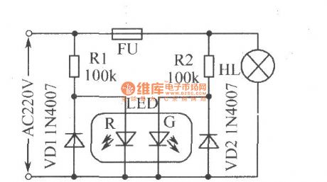
The blown fuse indicator circuit is shown as the figure. The LED -R is used to the AC power indicator, andLED -G is used the fuse FU status indicator. When FU is normal, two LEDs arelit,and the light isorange; after FU fuses, LED -G turns off, and only LED -R emits red light. The current limiting resistors R10, R2 can be replaced by the 220nF/450V capacitor,then the VD1, VD2 can be eliminating.
(View)
View full Circuit Diagram | Comments | Reading(2761)
BA313 sound recording or reproducing circuit diagram with ALC
Published:2012/7/16 3:15:00 Author:Ecco | Keyword: sound recording, reproducing , ALC
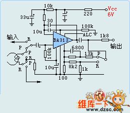
BA313 is a sound recording and preamplifier circuit with built-in automatic level control circuit (ALC), and it is commonly used in the cassette tape recorder. It is available in 9 -pin DIP dual in-line package. The circuit has the following characteristics : automatic level control with a wide range, wide working voltage range ( 3-12V ), high gain, low distortion, low noise.
(View)
View full Circuit Diagram | Comments | Reading(3435)
Impedance matching circuit diagram
Published:2012/7/11 2:07:00 Author:Ecco | Keyword: Impedance matching
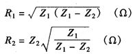
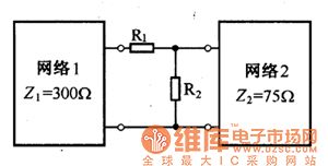
Figure 1 shows the impedance matching attenuator composed of resistor, andit is connectedbetween two networks with different impedance characteristic to play the role of matched impedance .Matching resistance in the devicecan be determined by following formula:
Z1 and Z2 areimpedance of the network 1 and network 2 , when they are respectively substituted into the above two formulas , then R1 = 259.8Ω, the R2 = 86.6Ω.
(View)
View full Circuit Diagram | Comments | Reading(994)
DC low-voltage blown fuse indicator circuit diagram
Published:2012/7/11 1:54:00 Author:Ecco | Keyword: DC low-voltage , blown fuse indicator

DC low-voltage blown fuse indicator circuit is shown as Figure 1, which consists of two light-emitting diodes VD2 , VD3 , a silicon rectifier diode VD1 and resistor R. When the fuse is good, the green light-emitting diode VD3 is bright. As the function of VD1 and VD3, the two ends' level of VD2 is equipotential, the red light-emitting diode VD2 is turned off. When the fuse is blown, VD3 it turned off as the cathode has no voltage, then the red light-emitting diode VD2 emits light as the influence of VD1 and R. According to the switching of VD2 and VD3, people can easily judge on-off status.
(View)
View full Circuit Diagram | Comments | Reading(2793)
High-power Darlington internal circuit diagram
Published:2012/7/8 21:55:00 Author:Ecco | Keyword: High-power Darlington

Ordinary Darlington's DC magnification hFE is particularly high, so it is used normally only below 2W. When the power increases, the tube's pressure drop make temperature increase, pre- transistor leakage current will be gradually enlarged, resulting in the deterioration of the overall thermal stability. In order to overcome this deficiency, the high-power Darlington is set balanced resistor, and it is also connectrd a freewheel diode VD between C and E reverse to make over-voltage protection. When the inductive load ( relay coil ) is suddenly cut off, VD can release the reverse voltage to prevent the breakdown of the internal transistor. Figure a shows the internal circuit of high-power PNP Darlington, and Figure b shows the internal circuit of NPN type high-power Darlington.
(View)
View full Circuit Diagram | Comments | Reading(1055)
Transistor radio tuning instruction circuit diagram
Published:2012/7/5 20:37:00 Author:Ecco | Keyword: Transistor radio, tuning instructions

The transistor radio tuning instruction circuit is shown in Figure 1 . When the tuner is accurate, the AGC voltage is minimum, and the emitter current of VT1 is minimum, and emitter voltage drop is also minimum, VT2's emitter current is minimum, then the light emitted by light-emitting diode VD is darkest; conversely, if the tuning is offset, light-emitting diode's light is enhanced. So it can be accurately tuned according to this characteristic.
(View)
View full Circuit Diagram | Comments | Reading(2041)
Pulse discrimination circuit diagram
Published:2012/7/5 21:02:00 Author:Ecco | Keyword: Pulse discrimination

Figure 1 is a pulse discrimination circuit diagram composed of color light-emitting diodes. When the positive pulse arrives , VT1 is breakover, then color light - emitting diode VD1 emits green light; VT2 is breakover when there's no pulse, the color light-emitting diode VD1 emits red light . And people can distinguish the presence or absence of pulse according to this.
(View)
View full Circuit Diagram | Comments | Reading(809)
Basic inverting integrator circuit diagram
Published:2012/7/1 20:19:00 Author:Ecco | Keyword: inverting integrator

The integrator circuit consists of operational amplifiers and resistors, capacitors. The operational amplifier incircuit can be selectedaccording to the computing precision, but the circuit 's output voltage and current should not exceed the rated output value of the op amp, Vom and Iom.
(View)
View full Circuit Diagram | Comments | Reading(730)
SN75490 thermal print head driver circuit diagram
Published:2012/7/1 20:35:00 Author:Ecco | Keyword: thermal, print head driver

SN75490 is used to drive many commonly used thermal print head, and it contains six AND gate drivers with common strobe pulse. Each driver has a totem pole output, and the calibration output voltage range is 4.75 ~ 3.5V, input side is compatible with TTL and 5V CMOS, and the power supply current capacity is 30mA . Absorption current capacity is 50mA, and the standard supply voltage is ±5V, it has strobe input end.
(View)
View full Circuit Diagram | Comments | Reading(2111)
The integrator (LM318) circuit diagram with expanded timing range
Published:2012/7/1 20:27:00 Author:Ecco | Keyword: integrator, expanded timing range

The integrator can easily work with a very short and very long time constant. The integration time constant is ( R2/R1) RC , if the precision of resistors R1 , R2 is ± 0.1 % , you can get a very good linearity . The advantages of this circuit are: it is easy to adjust its initial state because the capacitor is grounded with one end. If the switch is grounded at one end, the output is zero when switch is closed, the initial state is zero ; If one end of switch is connected to voltage V1, the initial state is V1. The integration period of the circuit can be as short as 1ns or as long as 1000s. The bandwidth of the integrator depends on the characteristics of the op amp. The integrator composed of LM318 and CA3100 op amps is suitable for high frequency signal points.
(View)
View full Circuit Diagram | Comments | Reading(1545)
DS2762 pin array diagram
Published:2011/12/2 0:33:00 Author:May | Keyword: land patten
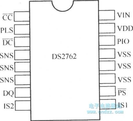
DS2762 is lithium ion battery monitor chip. It is produced by Maxin company. It can real-time monitor the parameter of voltage, current, charge and discharge condition and dump energy, etc. The chip can store this data. The chip can provide this data to SCM. And SCM can do relvant treat to the data. DS2762 chip cancollect data, store information. DS2762 chip hasthe features of functional integrity, external wiring simple and so on. Its pin array is shown in the following diagram.
(View)
View full Circuit Diagram | Comments | Reading(1370)
The combination sine wave circuit of 400Hz LED and operational amplifier
Published:2011/11/10 0:09:00 Author:May | Keyword: sine wave, LED, operational amplifier, 400Hz

In dimensional calculation bridge circuit, LED with norlinear resistor usage and operational amplifier are used in combination, and the power supply voltage is 15V. If R,C values change, this circuit can work at other frequency. R can adjust output width and its range is 10~20Vp-p, and the circuit total harmonic distortion is 1%.
(View)
View full Circuit Diagram | Comments | Reading(1497)
2-10 system decoding circuit
Published:2011/12/1 20:30:00 Author:May | Keyword: 2-10 system, decoding

RS7447 BCD code to seven-segment decoder can provide seven segment common anode digisplay. Binary system input pointer consists of RS7404 six inverter and four LED. It shows that input end uses binary system form to express ten's digit. It is suited to teach experiment.
(View)
View full Circuit Diagram | Comments | Reading(2075)
Four-stage Bessel low pass filter circuit diagram
Published:2011/7/28 0:45:00 Author:Nicole | Keyword: four-stage Bessel, low pass filter

View full Circuit Diagram | Comments | Reading(4518)
Image interface circuit
Published:2011/8/10 3:58:00 Author:Nicole | Keyword: image
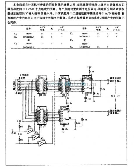
This circuit is used between computer and ordinary cathode ray oscillograph, the oscillograph phosphor screen displays an image composed of 512*512 dots, the image is stored in computer memory. The position of each dot is limited by two voltages, those voltages are transported to the V input terminal and H input terminal of cathode ray oscillograph. Two binary data words is fed to two A/D converter by computer, the voltage produced by converter is proportional to the value of these data words. These dots repeated display many times per second, so the produced image will not flash. (View)
View full Circuit Diagram | Comments | Reading(624)
An example of LM317T application circuit
Published:2011/8/10 4:03:00 Author:Nicole | Keyword: application circuit
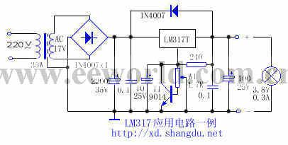
The load of this adjustable regulated power supply which is produced by LM317T is always damaged due to the output voltage rises which is caused by potentiometer's poor contact. If adding a triode(as shown in the figure) under normal circumstances, T1's base level is 0, T1 turns off, it has no influence on circuit; when the W1 is poor contact, T1's base current rises, when it rises to 0.7V, T1 turns on, it makes the regulation terminal voltage of LM317T drop, the output voltage drops too, then to protect the load. If it removes the triode, and cuts W1 connection conter point, 3.8V bulb is burned down immediately, the output voltage reaches 21V. When it is added T1, the brightness of bulb reduces, then the LM317T output voltage is only 2V, it can effectively protect load.
(View)
View full Circuit Diagram | Comments | Reading(2639)
Unfired bricks moisture detector 3
Published:2011/8/10 4:12:00 Author:Nicole | Keyword: Unfired brick, moisture detector
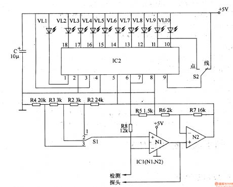
This unfired bricks moisture detector circuit is composed of detection input circuit and LED display circuit, it is shown in the figure 8-77.
The detection input circuit iscomposed of detector probe, operation amplifier integrated cirucit IC1(N1, N2), resistors R1-R8 and water content measurement area selection switch S1.
LED display circuit consists of LED linear analogue display drive integrated circuit IC2, LED VL1-VL10 and point/line display selection switch S2.
S1 has three shifts, 1 shift tests 13% water content area, 2 shift tests 14% water content area, 3 shift tests 15% water content area.
(View)
View full Circuit Diagram | Comments | Reading(1335)
8w fluorescent light electronic ballast circuit
Published:2011/8/22 21:13:00 Author:muriel | Keyword: 8w , fluorescent light , electronic ballast
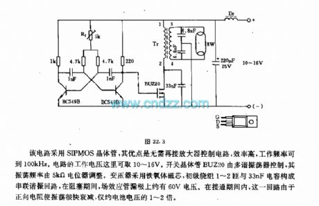
The circuit uses SIPMOS transistors, the advantages of itare control circuit without amplifier, high efficiency, operating frequencycan achieve 100kHz. The voltage of circuit can be10~16V. Switching transistor BUZ20 is controlled by the multivibrator, the oscillation frequency isadjusted by the 5kΩ potentiometer. Transformer with ferrite core, primary winding 1-2 turns and the 33nF capacitorformthe series resonant circuit, when it is blocking, the FET drain voltage is about 60V. In the connected period, the forward resistance of the circuit makes oscillations quickly decay, only about 1~2 times of the battery voltage.
(View)
View full Circuit Diagram | Comments | Reading(3418)
High resistance power distribution circuit
Published:2011/8/22 20:58:00 Author:muriel | Keyword: High resistance, power distribution circuit
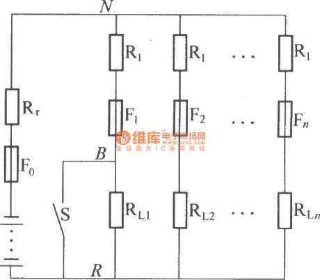
The figure is a circuit diagram of high resistance power distribution. The marked differencebetween it and DZL power distribution is the current limiting resistor R1 which tandem connection specific contact resistance in every shunt load, the general value is 5 times to 10 times of battery internal resistance. If one of the shunts short circuiting, because of the R1 limiting short-circuit current, at the same time the L×di/dt is lesser too. As shown is the voltagechange schematic diagram between N and R. The R1 and Re can make the change of voltagebetween N and R which isallowed in theerror rangeofpower supply system , it makes the loads in the system mutual independence.
(View)
View full Circuit Diagram | Comments | Reading(768)
DZW75-48/5050II high frequency rectifier filter circuit
Published:2011/12/4 20:45:00 Author:May | Keyword: high frequency reetifier, filter
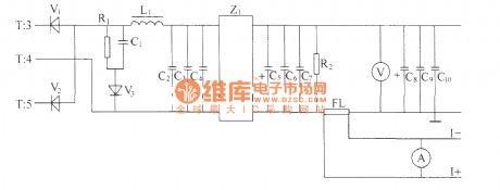
Alternating positive and negative pulse voltage of high-frequency transformer T's secondary induction is rectified by the full-wave rectifier composed of high-power high frequency switching diodes V1,V2, then it is smoothed filtered by L filter composed of inductor and capacitors C2, C3, C4 and Z1 power filter, then it gets 48V volts d.c. output with met the index high and low frequency noise requirements at output end. Impulse width determines the height of output voltage directly. Impulse width is wide, and output voltage is high, impulse width is narrow, output voltage is low. The output end is connected a voltmeter in order to measure display output volts d.c. R2 is leak resistor, and FL is current divider.
(View)
View full Circuit Diagram | Comments | Reading(2494)
| Pages:89/471 At 2081828384858687888990919293949596979899100Under 20 |
Circuit Categories
power supply circuit
Amplifier Circuit
Basic Circuit
LED and Light Circuit
Sensor Circuit
Signal Processing
Electrical Equipment Circuit
Control Circuit
Remote Control Circuit
A/D-D/A Converter Circuit
Audio Circuit
Measuring and Test Circuit
Communication Circuit
Computer-Related Circuit
555 Circuit
Automotive Circuit
Repairing Circuit