
Index 170
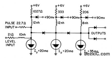
TUNNEL_DIODE_OR_GATE
Published:2009/7/16 2:08:00 Author:Jessie
Uses two cascaded monostables.- Transistor Manual, Seventh Edition, General Electric Co., 1964, p 370. (View)
View full Circuit Diagram | Comments | Reading(616)
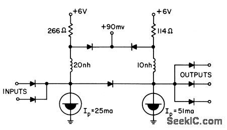
TUNNEL_DIODE_AND_GATE
Published:2009/7/16 2:05:00 Author:Jessie

Three cascaded monostables provide adequate gain for high-speed computer and logic.- Transistor Manual, Seventh Edition, General Electric Co., 1964, p 370. (View)
View full Circuit Diagram | Comments | Reading(997)
PREFERRED_VARIABLE_GATE_GENERATOR
Published:2009/7/16 2:04:00 Author:Jessie
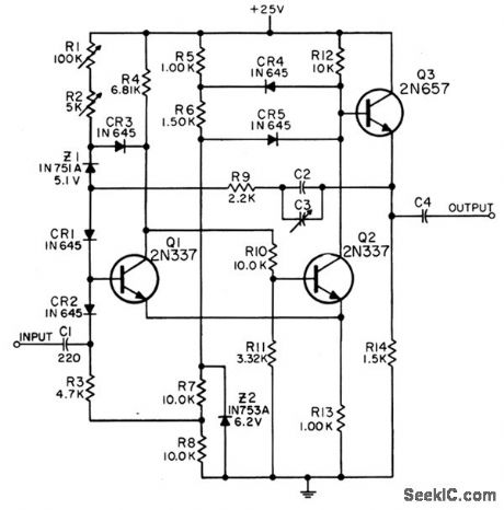
Uses multivibrator to generate rectangular gate waveform whose duration is directly proportional to setting of potentiometer and is relatively independent of temperature effects. Used to produce movable markers for radar displays. Input signal is negative, from 10 to 20 V. Output is 12.5 V, with gate width adjustable from 10 to 10,000 microsec by changing values of R1 and C2.-NBS, Handbook Preferred Circuits Navy Aeronautical Electronic Equipment, Vol. II, Semiconductor Device Circuits, PSC 16 (originally PC 252), p 16-2. (View)
View full Circuit Diagram | Comments | Reading(515)
UJT_TRIGGERED_CROWBAR
Published:2009/7/13 21:25:00 Author:May
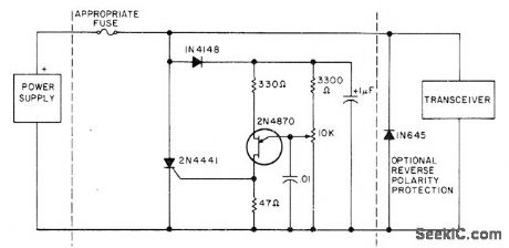
Circuit is used between transceiver and regulated 12-V power supply to protect transceiver from overvoltage or reverse polarity UJT permits precise setting of overvoltage level at which 2N4441 SCR crowbar operates. Fuse is blown within microseconds of overvoltage. Crowbar can be built into transceiver.-Circuits, 73Magazine, July 1977, p35. (View)
View full Circuit Diagram | Comments | Reading(1329)
FAST_TUNNEL_DIODE_GATE
Published:2009/7/16 2:03:00 Author:Jessie
At coincidence between sampling pulse at one input and 100-Mc block pulse at other input, 11 ma current through D3 switches D3 to high level, making D4 pass current to load.-A. A. Fleischer and E. Johnson, New Digital Conversion Method Provides Nanosecond Resolution, Electronics, 36:18, p 55-57. (View)
View full Circuit Diagram | Comments | Reading(545)
CERAMIC_FILTER_DRIVE
Published:2009/7/13 21:22:00 Author:May

National LM3011 gain block provides three differential stages and current-source output suitable for driving 300-ohn,ceramic filter in IF amplifier of FM receivel,Circuit provides 60 dB of power gain to matched load.-''Audio Handbook,''National Semiconductor,Santa Clara,CA,1977,p 3-11-3-12. (View)
View full Circuit Diagram | Comments | Reading(719)
MECHANICAL_COUNTER_SPEEDUP
Published:2009/7/13 21:22:00 Author:May
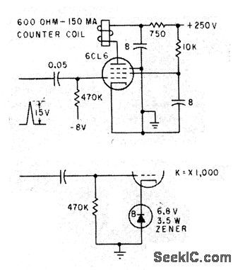
Vacuum-tube circuit doubles speed of counter, with minimum of overheating and other damage to counter coil and mechanism. Operation depends on pulsed overvolting for a limited time, along with some sliding overvolting wherein excess voltage is applied to coil when circuit is first completed, then reduced so it drops below normal operating voltage during pull-in time.-R. L. Ives, Circuit Modifications for Boosting Counter Speed, Electronics, 33:7, p112-114. (View)
View full Circuit Diagram | Comments | Reading(573)
TRIAC_DRIVE
Published:2009/7/13 21:20:00 Author:May
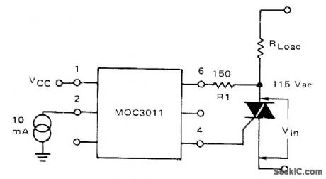
Motorola MOC3011 optoisolatoR serves as interface between 10-mA input circuit and gate of triac controlling AC load. Choice of triac depends on load being handled. Optoisolator detector chip responds to infrared LED; once triggered on, optoisolator stays on until input current drops below holding value of about 100μA.-P. O'Neil, Applications of the MOC3011 Triac Driver, Motorola, Phoenix, AZ, 1978, AN-780, p 2. (View)
View full Circuit Diagram | Comments | Reading(2651)
BASIC_PNP_GATE
Published:2009/7/16 2:02:00 Author:Jessie
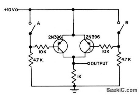
Circuit is and gate if closing of switch is an input, Circuit is or gate if opening of switch is an input. Provides phase inversion of input without complicating overall circuitry.- Transistor Manual, Seventh Edition, General Electric Co., 1964, p 176. (View)
View full Circuit Diagram | Comments | Reading(649)
VOX__FOR_SSB
Published:2009/7/13 21:20:00 Author:May
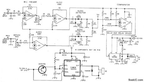
Uses LM3900 quad Norton opamp and NE555 timer operating from single supply. U1A and U1B amplify microphone signal. U1C amplifies audio sample obtained from station loudspeaker. Outputs of both amplifiers are converted to varying DC voltages by rectifiers in detector stages. Rectifier outputs are summed resistively by R6 and R7 for application to inverting input of voltage comparator U1D. Positive microphone signal drives comparator output low and triggers NE555, which in turn energizes 12-V relay K1 after delay set at about 10 ms by R8 to avoid losing first syllable. Same delay applies to relay dropout, to hold relay closed between words. If K1 drops out for fraction of second at end of timing cycle even though audio is present, add 2N5139 transistor to NE555 input as shown.-D. A. Blakeslee, A VOX for a Very Small Box, QST, March 1976, p 24-26. (View)
View full Circuit Diagram | Comments | Reading(1066)
PULSE_HEIGHT_TO_WIDTH_CONVERTER
Published:2009/7/16 2:02:00 Author:Jessie

Converts 0 to 2-V pulse to gate for pulse height to pulse width conversion. Gate width, directly proportional to data pulse amplitude, is applied to dock circuits.-W. W. Grannemann et al., Pulse-Height-to-Digital Signal Converter, Electronics, 33:2, p 58-60. (View)
View full Circuit Diagram | Comments | Reading(1272)
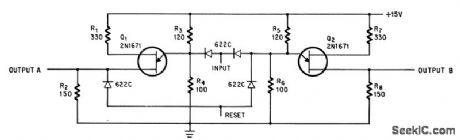
GATED_MVBR
Published:2009/7/16 2:01:00 Author:Jessie
Complementary pulse trains appear at outputs 1 and 2 when gate is applied.-R. Newmeyer, Gated Multivibrator Output Provides Constant Pulse Width, Electronics, 38:26, p 69. (View)
View full Circuit Diagram | Comments | Reading(614)
ANALOG_GATE
Published:2009/7/16 2:00:00 Author:Jessie
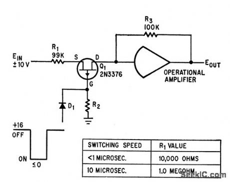
Output is -10.0025 V for +10 V input, and +9.9975 V for -10 V input.-M. Shipley Sr., Analog Switching Circuits Use Field-Effect Devices, Electronics, 37:32, p 45-50. (View)
View full Circuit Diagram | Comments | Reading(654)
BRIDGE_GATE_WITH_TOROID
Published:2009/7/16 1:59:00 Author:Jessie
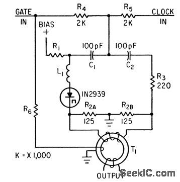
Portion of gate input signal is fed to wire threading output toroid, to cancel output spike of ac bridge.-F. W. Kantor, Tunnel-Diode Gate has Sub-nanosecond Rise Time, Electronics, 35:15, p 62-64. (View)
View full Circuit Diagram | Comments | Reading(544)
FM_DEMODULATOR
Published:2009/7/13 21:17:00 Author:May
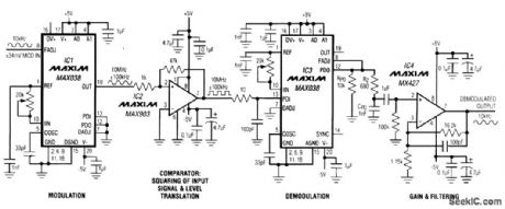
The frequencies at IC3's phase-detector output are the sum and difference of the frequencies at PDI and OUT. Thus, with appropriate cutoff frequency and gain, the low-pass filter (IC4) passes only the original 10-kHz signal to the demodulated output. The pole for this filter is set by the 16.2-kΩ and 100-pF components. The frequency response for IC3's PLL is set by RPD, CPD, and RZ, When the loop is in lock, PDI is in approximate phase quadrature with the output signal. Also, when in lock, the duty cycle at PDO is 50 percent, and PDO's average output current is 250 μ A. The current sink at FADJ demands a constant 250 μ A, so PDO outputs above and below that level develop a bipolar error voltage across RPD that drives the FADJ voltage input. Note: The MAX038's internal phase detector is a phase-only detector, producing a PLL whose frequency-capture range is limited by the bandwidth of its loop filter. For wider-range applications, consider an external phase-frequency detector. (View)
View full Circuit Diagram | Comments | Reading(0)
NOR_LOGIC_USING_SERIES_TRANSISTORS_FOR_AND_GATE
Published:2009/7/16 1:59:00 Author:Jessie

Requires inverter at output.- Transistor Manual, Seventh Edition, General Electric Co.,1964, p 179. (View)
View full Circuit Diagram | Comments | Reading(605)
FOUR_DIODE_TR_SWITCH
Published:2009/7/13 21:17:00 Author:May
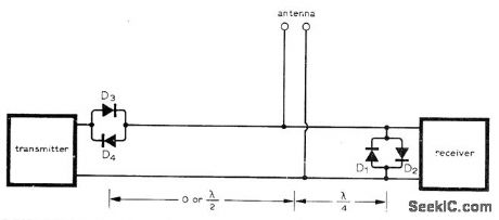
Circuit requires only two pairs of high-frequency switching diodes having current ratings appropriate for transmitter power. With diode pairs spaced as shown, impedance at T junction looking toward transmitter is infinite during reception because there is open circuit half a wavelength away created by nonconducting D3 and D4. Line is matched in receiver direction so all incoming power from antenna goes into receiver. When transmitter is on, D3 and D4 conduct and power flows toward antenna, while D1 and D2 also conduct and place short-circuit across receiver input.-A. Lieber, Passive Solid-State Antenna Switch, Wireless World, Jan. 1975, p 12. (View)
View full Circuit Diagram | Comments | Reading(710)
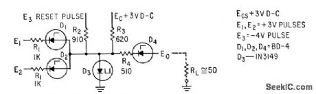
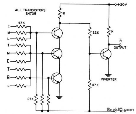
THREE_STATE_LOGIC
Published:2009/7/16 1:56:00 Author:Jessie
With no input pulse (state 1), output A is zero and output B is 1.5 v. With a positive input pulse (state 2),A and B are both 1.5 v. With a negative input pulse (state 3), A and B are both zero. A 12-v positive pulse at the reset terminal restores stale 1.-S. F. Summer, Two Unijunction Transistors Produce Three-State Circuit, Electronics, 39:1, p 100. (View)
View full Circuit Diagram | Comments | Reading(525)
TRIAC_CONTROL_WITH_OPTOISOLATOR
Published:2009/7/13 21:17:00 Author:May
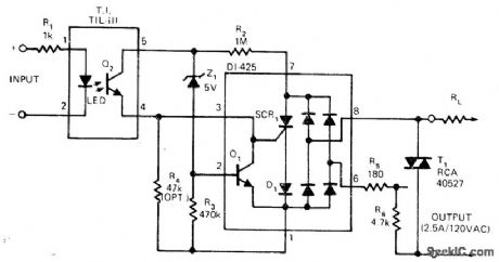
Dionics D1425 switchable bridge circuit controls 120-VAC line in optically isolated zero-crossing solid-state relay that can be used as trigger form power triac. Small AC devices, drawing under 5 W, can be switched directly in either random or zero-crossing mode.-High-Voltage Monolithic Technology Produces 200V AC Switching Circuit, EDN Magazine, April 5, 1975, p 121. (View)
View full Circuit Diagram | Comments | Reading(2936)
SHIFT_REGISTER
Published:2009/7/13 21:17:00 Author:May

Memory chain of 16 miniature logic tubes (three shown) serves as counter for weighing and batching.-M. E. Bond, Cold-Cathode Tubes as Triggers, Electronics, 38:7, p 76-85 (View)
View full Circuit Diagram | Comments | Reading(0)
| Pages:170/471 At 20161162163164165166167168169170171172173174175176177178179180Under 20 |
Circuit Categories
power supply circuit
Amplifier Circuit
Basic Circuit
LED and Light Circuit
Sensor Circuit
Signal Processing
Electrical Equipment Circuit
Control Circuit
Remote Control Circuit
A/D-D/A Converter Circuit
Audio Circuit
Measuring and Test Circuit
Communication Circuit
Computer-Related Circuit
555 Circuit
Automotive Circuit
Repairing Circuit