
Amplifier Circuit
Index 85
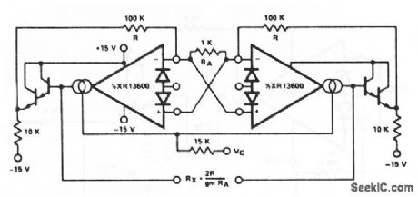
Multiplexer
Published:2009/7/17 3:34:00 Author:Jessie
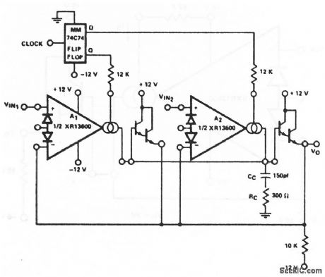
This circuit uses two sections of an XR-13600 (Fig.11-1B) and a standard flip-flop to form a multiplexer. The maximum clock rate is limited to about 200 kHz, with a maximum input differential of 5V. EXAS corporation Databook 1990 p 5-256 (View)
View full Circuit Diagram | Comments | Reading(946)
Servo_motor_preamplifier
Published:2009/7/17 3:30:00 Author:Jessie
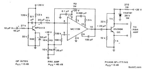
Servo motor preamplifier (courtesy Motorola Semiconductor Products Inc.). (View)
View full Circuit Diagram | Comments | Reading(666)
Line_operated_servo_motor_amplifier
Published:2009/7/17 3:29:00 Author:Jessie
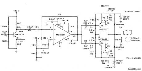
Line-operated servo motor amplifier (courtesy Motorola Semiconductor Products Inc.). (View)
View full Circuit Diagram | Comments | Reading(1823)
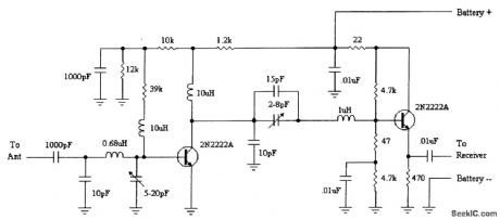
TWO_TRANSISTOR_TRF_RADIO_RECEIVER_WITH_AUDIO_AMPLIFIER
Published:2009/7/17 3:28:00 Author:Jessie
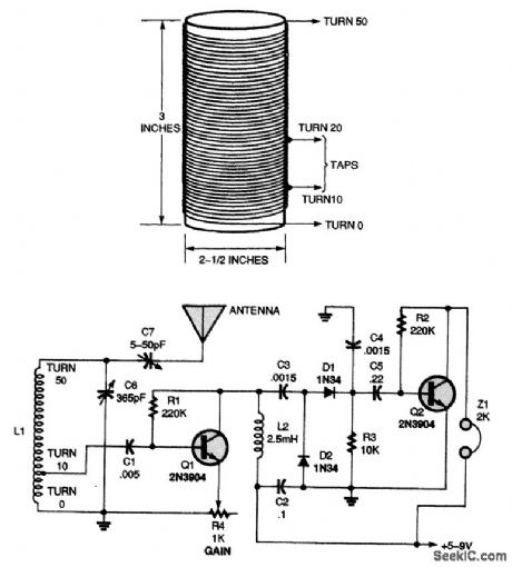
This receiver allows you to select the gain of its 11 RF ramplifier by adjusting R4. (View)
View full Circuit Diagram | Comments | Reading(5442)
Servo_motor_power_amplifier
Published:2009/7/17 3:27:00 Author:Jessie
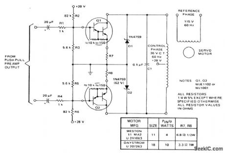
Servo motor power amplifier (courtesy Motorola Semiconductor Products Inc.). (View)
View full Circuit Diagram | Comments | Reading(1095)
Single_amplifier_VC0
Published:2009/7/17 3:26:00 Author:Jessie
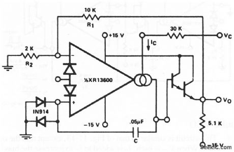
This circuit uses only one section of an XR-13600 (Fig.11-1B) to form a VCO. The remaining section can then be used for another purpose. EXAR Corporation Databook 1990 p 5-255 (View)
View full Circuit Diagram | Comments | Reading(561)
Sinusoidal_VCO
Published:2009/7/17 3:23:00 Author:Jessie
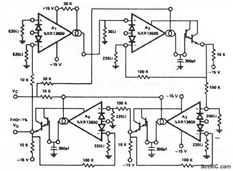
This circuit amplifiers configured as uses two XR-13600 OTAs (Fig.11-1B) , with three of the amplifiers configured as low-pass filters and the fourth as a limiter/inverter. The circuit oscillates at the frequency, where the loop phase-shift is 360° or 180°for the inverter and 60° per filter stage. This VCO operates from 5 Hz to 50 kHz with less than 1 % THD. EXAR corporation Databook, 1990 p 5-255 (View)
View full Circuit Diagram | Comments | Reading(870)
Ramp_pulse_VCO
Published:2009/7/17 3:22:00 Author:Jessie
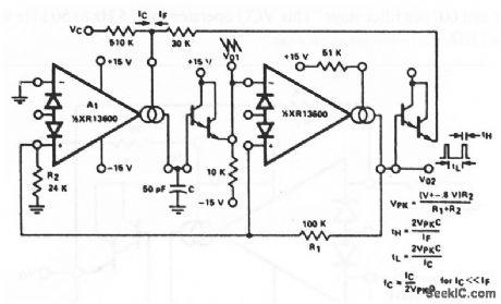
This circuit is similar to that of Fig. 11-13, except that the outputs are ramps and pulses. When V02 is high, IF is added to IC to increase the bias current of amplifier A1, and thus to increase the charging rate of capacitor C. When V02 is low, IF goes to zero and the capacitor discharge current is set by IC, EXAR Corporaton Databook 1990 p 5-255 (View)
View full Circuit Diagram | Comments | Reading(775)
R_C_RECEIVER_PREAMPLIFIER
Published:2009/7/17 3:18:00 Author:Jessie
The circuit shown is small, draws little current, and is easily fabricated on a perfboard-just keep the wires short and the bypass capacitors close to their position on the schematic. To install, make a break in the wire from the antenna and insert the preamplifier. With proper trimming, this circuit yields about 20 dB of gain. (View)
View full Circuit Diagram | Comments | Reading(739)
Frequency_shift_keyer_using_the_MC1545G_wide_band_amplifier_
Published:2009/7/17 3:09:00 Author:Jessie
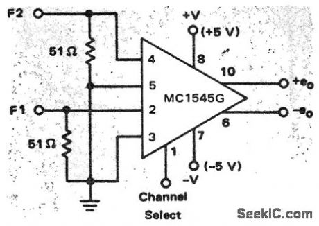
Frequency shift keyer using the MC1545G wide-band amplifier (courtesy Motorola Semiconductor Products Inc.). (View)
View full Circuit Diagram | Comments | Reading(582)
NARROW_BAND_RADAR_AMPLIFIER
Published:2009/7/17 3:09:00 Author:Jessie
Twin-tee feedback loop tuned to modulating frequency between 60 and 400 cps is used with video crystal and chopper of low-cost c-w radar receiver. Minimum detectable level is -55 dbm.-R. Fleming, Modulation Techniques Cut Radar Cost, Electronics, 35:35, p 56-58. (View)
View full Circuit Diagram | Comments | Reading(1043)
Floating_voltage_controlled_resistor
Published:2009/7/17 3:08:00 Author:Jessie
This circuit is similar to that of Fig. 11-6, except that both sections of the XR-13600 (Fig. 11-1B) are used. Each end of the resistor can be at any voltage within the output range of the XR- 13600. EXAR Corporation Databook 1990 p 5-254 (View)
View full Circuit Diagram | Comments | Reading(654)
MATCHING_OPAMPS
Published:2009/7/11 1:43:00 Author:May
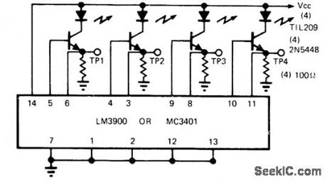
Simple circuit checks condition of quad Norton opamps (Nationai LM3900 or Motorola MC3401). Can also be used to match or select devices for similar DC characteristics in critical applications. Amplifier under test is plugged into socket connected as shown. Good unit makes all four LEDs glow with about same brightness, and all four testpoint voltages will agree within about 2 mV. If one section of amplifier is damaged, associated LED will glow very brightly or not at all. Wide variations between test-point voltages indicate partial damage. For critical applications, select amplifiers by matching average test-point voltages.-R. Tenny, Check Norton Amplifiers Quickly, EDNMagazine, March 5, 1974, p 72. (View)
View full Circuit Diagram | Comments | Reading(984)
CLOCK_PULSE_AMPlJFlER
Published:2009/7/11 1:33:00 Author:May
Genercates clock pulses for driving all flip-flops in magnetic drum timing channel system, and generates digit square-wave signals used in Manchester conversion network of writing amplifer. External signal generator provides desired frequency for time track.-A.j. Strassman and R.E. Keeter, Clock Track Recorder For Memory Drum, Electronics, 32:41, p74-76. (View)
View full Circuit Diagram | Comments | Reading(687)
DELAY_LINE_AMPLIFIER_FOR_CLUTTER_SIMULATOR
Published:2009/7/17 3:03:00 Author:Jessie
Used with ultrasonic delay line and 30-Mc Gaussian noise source to simulate actual clutter received during consecutive radar sweeps. Input 1 is amplified version of delay line output signal, which is added to noise input 2 in common plate load of V1 and V2, for amplification by V3. These three tubes together with tuned input to delay line form staggered Butterworth triple centered on 30 Mc, with half-power band-width of 2.75 Mc. Third input permits insertion of pulse for precise synchronizing lo repetition frequency of clutter simulator.-J. Atkin, H. J. Bikel, and M. Weiss, Realistic Simulation of Radar Clutter, Electronics, 32:39, p 78-81. (View)
View full Circuit Diagram | Comments | Reading(801)
High_speed_integrator_using_an_ECG915_operational_amplifier
Published:2009/7/17 3:02:00 Author:Jessie
High-speed integrator using an ECG915 operational amplifier (courtesy GTE Sylvania Incorporated). (View)
View full Circuit Diagram | Comments | Reading(759)
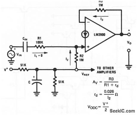
Norton_inverting_ac_amplifier_with_NVSUBBE_SUB_biasing
Published:2009/7/17 4:11:00 Author:Jessie

This circuit shows both an inverting ac amplifier and a third method for biasing. The input bias voltage VBE establishes a current through R3 to ground, This current comes from the amplifier output, so VO must rise to a level that causes the current to flow through R2. VO is calculated from the ratio of R2 and R3, as shown by the equations. When this NVBE biasing is used, R1 and R2 are established first, then R3 is added for the desired VO. National Semiconductor Linear Applications Handbook 1991 P220 (View)
View full Circuit Diagram | Comments | Reading(701)
BAXANDALL_TONE_CONTROL_AUDIO_AMPLIFIER
Published:2009/7/11 1:12:00 Author:May
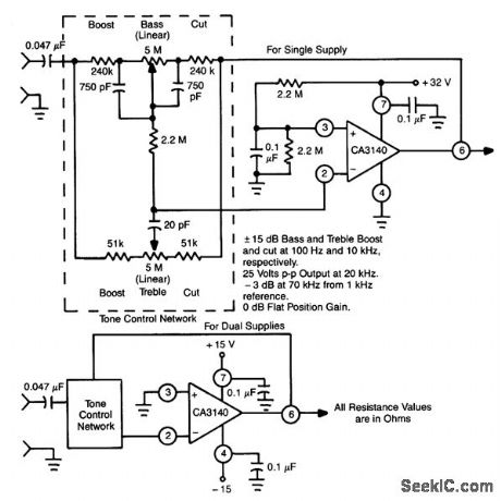
This circuit exploits the high slew rate, high input impedance, and high output-voltage capability of CA3140 BiMOS op amp. It also provides mid-band unity gain with standard linear potentiometers. (View)
View full Circuit Diagram | Comments | Reading(925)
Norton_noninverting_ac_amplifier_with_voltage_reference_biasing
Published:2009/7/17 4:10:00 Author:Jessie
This circuit shows both a noninverting ac amplifier and a second method for dc biasing. As in the case of the Fig. 11-32 circuit, the ac gain of this circuit is set by the ratio of the feedback resistor to the input resistor. However, the small-signal impedance of the internal diode at the (+) input must be added to the values of R1 when calculating gain, as shown by the equations. National Semiconductor Linear Applications Handbook, 1991, p 220, (View)
View full Circuit Diagram | Comments | Reading(691)
RADAR_POWER_AMPLIFIER
Published:2009/7/17 4:09:00 Author:Jessie
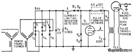
Handles pulses in range of 100 to 500 microsec at 2.2 Mc. Class B final stage Q2 delivers 105 w to piloading network serving as 5l-ohm load.-S. Horowitz and L. Humphrey, Satellite Sounder and Telemeter Chart Ionosphere Electron Density, Electronics, 34:25, p 50-53. (View)
View full Circuit Diagram | Comments | Reading(944)
| Pages:85/250 At 2081828384858687888990919293949596979899100Under 20 |
Circuit Categories
power supply circuit
Amplifier Circuit
Basic Circuit
LED and Light Circuit
Sensor Circuit
Signal Processing
Electrical Equipment Circuit
Control Circuit
Remote Control Circuit
A/D-D/A Converter Circuit
Audio Circuit
Measuring and Test Circuit
Communication Circuit
Computer-Related Circuit
555 Circuit
Automotive Circuit
Repairing Circuit