
Amplifier Circuit
Index 98
Low_noise_preamplifier_using_an_ECG1152_13_pin_module
Published:2009/7/20 3:21:00 Author:Jessie
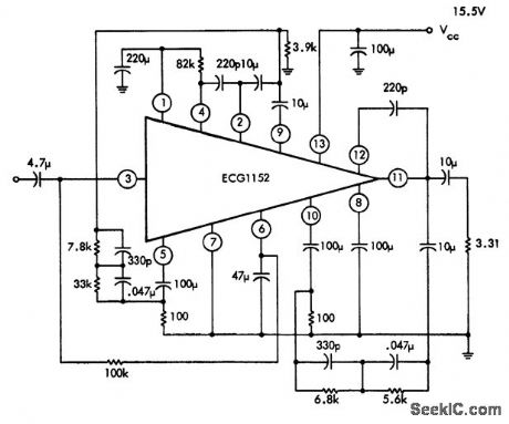
Low-noise preamplifier using an ECG1152 13-pin module. The ECG1152 is a dual two-stage direct-coupled amplifier. Typical voltage gain is 75 dB. Input resistance is 50K (courtesy GTE Sylvania Incorporated). (View)
View full Circuit Diagram | Comments | Reading(520)
OP_AMP_TESTER
Published:2009/7/20 3:15:00 Author:Jessie
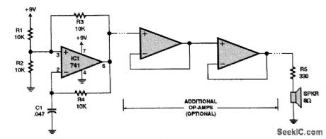
The circuit is a simple dead or alive test for an op amp. It is an oscillator that produces a 1500-Hz square wave, audible as a tone in the speaker. By looking at the output with an oscilloscope, you can measure the rise time. Several op amps can be tested at once by cascading them, as shown in the diagram. (View)
View full Circuit Diagram | Comments | Reading(1448)
Audio_amplifier_for_tape_recorder_using_an_EGG1043_14_pin_DIP
Published:2009/7/20 3:15:00 Author:Jessie
Audio amplifier for tape recorder using an EGG1043 14-pin DIP. Recommended supply voltage is 6 volts. Typical voltage gain is 85 dB. This circuit has an input impedance of 22K (courtesy GTE Sylvania Incorporated). (View)
View full Circuit Diagram | Comments | Reading(549)
OP_AMP_DC_OVERALL_FEEDBACK
Published:2009/7/20 3:15:00 Author:Jessie
Overall dc feedback stabilizes the whole amplifier. (View)
View full Circuit Diagram | Comments | Reading(502)
OP_AMP_DC_COUPLING_AND_OFFSET
Published:2009/7/20 3:14:00 Author:Jessie
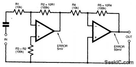
Dc interstage coupling might be tolerable in terms of offset errors (View)
View full Circuit Diagram | Comments | Reading(554)
1_watt_OTL_audio_power_amplifier_using_an_ECG1035
Published:2009/7/20 3:13:00 Author:Jessie
1-watt OTL audio power amplifier using an ECG1035. Packaging on the ECG1035 is a 12-pin plastic flat pack with metal tabs. Recommended supply voltage is 9 volts. Voltage gain is 50 dB. Frequency response is from 50 hertz to 100 kilohertz (courtesy GTE Sylvania Incorporated). (View)
View full Circuit Diagram | Comments | Reading(653)
OP_AMP_DC_FEEDBACK_STABILIZATION
Published:2009/7/20 3:13:00 Author:Jessie
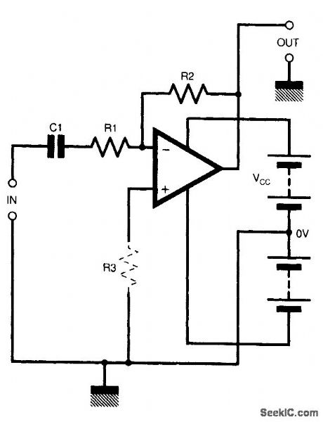
Blocking capacitor C1 ensures that dc negative feedback is maximized. (View)
View full Circuit Diagram | Comments | Reading(539)
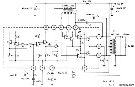
55_watt_OTL_audio_power_amplifier_using_an_ECG1037
Published:2009/7/20 3:12:00 Author:Jessie
5.5-watt OTL audio power amplifier using an ECG1037. Typical voltage gain is 55dB. Frequency response is from 30 hertz and 50 kilohertz. Input impedance is 36K (courtesy GTE Sylvania Incorporated). (View)
View full Circuit Diagram | Comments | Reading(556)
1_watt_audio_power_amplifier_using_an_ECG1033
Published:2009/7/20 2:59:00 Author:Jessie
1-watt audio power amplifier using an ECG1033. Supply voltage is 6 volts. Typical voltage gain at 1 kHz is 47 dB. Packaging for the ECG1033 is a 12-pin plastic pack with metal tabs (courtesy GTE Sylvania Incorporated). (View)
View full Circuit Diagram | Comments | Reading(595)
8_watt_AF_power_amplifier_for_8_ohm_or_4_ohm_speaker_load
Published:2009/7/20 2:53:00 Author:Jessie
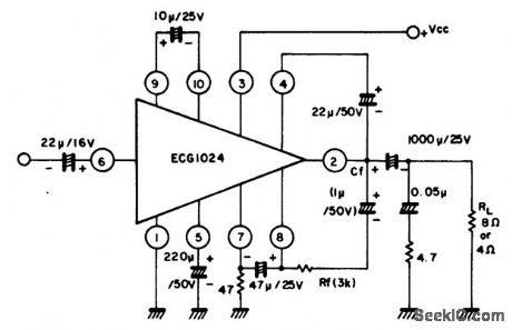
8-watt AF power amplifier for 8-ohm or 4-ohm speaker load. Typical supply voltage is 25 volts (courtesy GTE Sylvania Incorporated). (View)
View full Circuit Diagram | Comments | Reading(588)
4_watt_AF_power_amplifiers_for_low_cost_record_players_using_an_ECG1111_14_pin_DIP
Published:2009/7/20 2:52:00 Author:Jessie
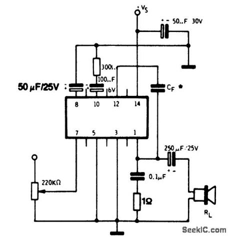
4-watt AF power amplifiers for low-cost record players using an ECG1111 14-pin DIP. The amplifier is designed to drive a 16-ohm load. Recommended supply voltage is 24 volts. Typical voltage gain is 74 dB. Input impedance is 110K, Capacitor CF can be either 510 pF or 820 pF, depending on the frequency response desired. For 510 pF the frequency response extends beyond 10 kHz. With CF at 820 pF the response falls off at about 8 kHz (courtesy GTE Sylvania Incorporated). (View)
View full Circuit Diagram | Comments | Reading(533)
2_watt_OTL_audio_power_amplifier_using_an_ECG1034
Published:2009/7/20 2:49:00 Author:Jessie
2-watt OTL audio power amplifier using an ECG1034. Recommended supply voltage is 12 volts. Typical voltage gain at 1 kHz is 50 dB. Input impedance is 20K. Frequency response is from 60 hertz to 50 kilohertz (courtesy GTE Sylvania Incorporated). (View)
View full Circuit Diagram | Comments | Reading(649)
1_watt_OTL_audio_power_amplifier_using_an_ECG1032
Published:2009/7/20 2:48:00 Author:Jessie
1-watt OTL audio power amplifier using an ECG1032. Typical voltage gain at 1 kHz is 50 dB (courtesy GTE Sylvania Incorporated). (View)
View full Circuit Diagram | Comments | Reading(505)
INVERTING_BISTABLE_BUFFER
Published:2009/7/9 22:02:00 Author:May
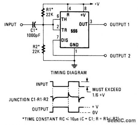
This circuit uses a 555 timer as a flip-flop bistable buffer. (View)
View full Circuit Diagram | Comments | Reading(617)
PRECISION_INCREASING_BUFFER
Published:2009/7/9 22:01:00 Author:May
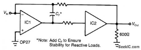
Adding an unity-gain buffer to your analog circuit can increase its precision. For example, by itself, the op amp IC1 exhibits a maximum dVOS/dT of 1.8 μA/℃ and can drive a 600-Ω load. Under thes, conditions, IC1 would dissipate 94 mW incrementally. Thus, the op amp's OJA of 150℃/W would change its VOS by 25μV.
The buffer, IC2, will isolate IC1 from the load and eliminate the change in power dissipation in IC1, thereby achieving 1C1's minimum, rated offset-voltage drive. The loop gain of IC1 essentially eliminates the offset of the buffer. Almost any unity-gain buffer will work, provided that it exhibits a 3-dB bandwidth that is at least 5 times the gain-bandwidth product of the op amp. (View)
View full Circuit Diagram | Comments | Reading(609)
OSCILLATOR_BUFFERS
Published:2009/7/9 21:58:00 Author:May
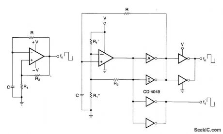
CM0S buffers added to an op amp oscillator improve performance, largely as a result of nonsymmetry and variability of the op amp's output saturation voitages. (View)
View full Circuit Diagram | Comments | Reading(784)
INSTRUMENTATION_AMPLIFIER
Published:2009/7/9 21:49:00 Author:May
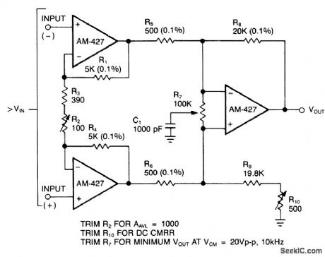
In a single difference amplifier Gonfiguration,the AM-427 exhibits common-mode rejection and spot noise voltage so low it is dominated by the resistor Johnson noise.The three-amplfier comfiguration shown avoids the low input-impedance characteristics of difference amplifiers.Because of the additional amplifiers used,the spectral noise volatge will increase from a typical of 3nV/Hz to approximately 4.9nV/Hz.The overall gain of the circuit is set at 1000;with balanced source resistors,a CMRR of 100dbis achieved. (View)
View full Circuit Diagram | Comments | Reading(0)
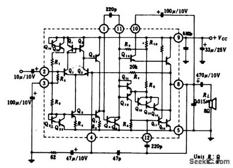
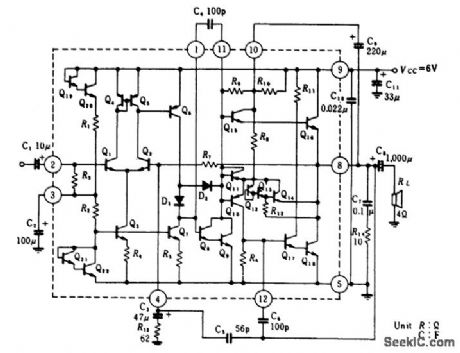
20_watt_single_ended_AF_power_amplifier
Published:2009/7/20 4:08:00 Author:Jessie
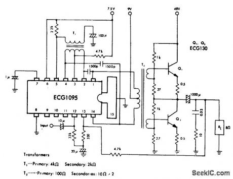
20-watt single-ended AF power amplifier. The ECG1095 is a 14-pin DIP with a tab and built-in AGC. The two output transistors are ECG130 bipolars (courtesy GTE Sylvania Incorporated). (View)
View full Circuit Diagram | Comments | Reading(621)
LOW_DRIFT_LOW_NOISE_dc_AMPLIFIER
Published:2009/7/9 21:42:00 Author:May
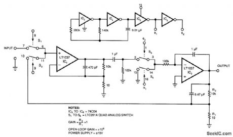
Figure 39-2's circuit combines a low-noise op amp, IC1, with a chopper-based carrier-modulation scheme to achieve a low-noise, low-drift dc amplifier whose performance exceeds any currently available monolithic amplifier. The amplifier's offset is less than 1μV/℃, and its drift is less than 0.05 μV. This circuit has noise within a 10-Hz bandwidth less than 40 nV. The amplifier's bias current, which is set by the bipolar input of IC1, is about 25 nA.
The 74C04 inverters (IC3 to IC6) form a simple 2-phase square-wave clock that runs at about 350 Hz.The complementary oscillator signals (Q1 and Q2) provide drive to S1 and S2,respectively, causing a chopped version of the input to appear at 101's input. IC1 amplifies this ac signal. S3 and S4 synchronously demodulate 101's square-wave output. Because 53 and 54 switch synchronously with S1 and S2, the cir-cuit presents proper amplitude and polarity information to IC2, the dc output amplifier. This output stage integrates the square wave to provide a dc voltage output. R1 and R2 divide the output and feed it back to the input chopper where the divided output serves as a zero signal reference. The ratio of RI and R2 sets the gain, in this case to 1000. (View)
View full Circuit Diagram | Comments | Reading(676)
65_watt_AF_power_amplifier_using_an_ECG1078_chip_powered_by_a_single_24_volt_supply
Published:2009/7/20 4:06:00 Author:Jessie
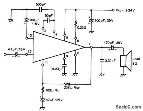
6.5-watt AF power amplifier using an ECG1078 chip powered by a single 24-volt supply. Frequency response is from 100 hertz to 20 kilohertz (courtesy GTE Sylvania Incorporated). (View)
View full Circuit Diagram | Comments | Reading(610)
| Pages:98/250 At 2081828384858687888990919293949596979899100Under 20 |
Circuit Categories
power supply circuit
Amplifier Circuit
Basic Circuit
LED and Light Circuit
Sensor Circuit
Signal Processing
Electrical Equipment Circuit
Control Circuit
Remote Control Circuit
A/D-D/A Converter Circuit
Audio Circuit
Measuring and Test Circuit
Communication Circuit
Computer-Related Circuit
555 Circuit
Automotive Circuit
Repairing Circuit