Want to post a buying lead? If you are not a member yet, please select the specific/related part number first and then fill the quantity and your contact details in the "Request for Quotation Form" on the left, and then click "Send RFQ".Your buying lead can then be posted, and the reliable suppliers will quote via our online message system or other channels soon.
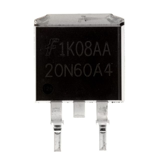
The HGT1S20N60A4S9A is MOS gated high voltage switching devices combining the best features of MOSFETs and bipolar transistors. These devices have the high input impedance of a MOSFET and the low on-state conduction loss of a bipolar transistor. The much lower on-state voltage drop varies only moderately between 25oC and 150.
This IGBT is ideal for many high voltage switching applications operating at high frequencies where low conduction losses are essential. This device has been optimized for high frequency switch mode power supplies.
Formerly Developmental Type TA49339.
HGT1S20N60A4S9A Maximum Ratings
HGT1S20N60A4S9A UNITS Collector to Emitter Voltage . . . . . . . . . . . . . BVCES 600 V Collector Current Continuous At TC = 25 . . . . . . . . . . . . . . . . . . . . . . . . . . . IC25 70 A At TC = 110 . . . . . . . . . . . . . . . . . . . . . . . . IC110 40 A Collector Current Pulsed (Note 1) . . . . . . . . . . . ICM 280 A Gate to Emitter Voltage Continuous. VGES ±20 V Gate to Emitter Voltage Pulsed . . . . . . . . . . VGEM ±30 V Switching Safe Operating Area at TJ = 150 (Figure 2) . . . . . SSOA 100A at 600V Power Dissipation Total at TC = 25 . . . . . . . . . . . . . . . . . . . . PD 290 W Power Dissipation Derating TC > 25 . . . . . . . . . . . . . . . . . . . . 2.32 W/ Operating and Storage Junction Temperature Range . . . . . TJ, TSTG -55 to 150 Maximum Lead Temperature for Soldering Leads at 0.063in (1.6mm) from Case for 10s. . . . . . . . . . . . . . . . TL 300 Package Body for 10s, See Tech Brief 334 . . . . . . . . . . . . . . . . TPKG 260 CAUTION: Stresses above those listed in "Absolute Maximum Ratings" may cause permanent damage to the device. This is a stress only rating and operation of the device at these or any other conditions above those indicated in the operational sections of this specification is not implied. NOTE: 1. Pulse width limited by maximum junction temperature.
HGT1S20N60A4S9A Features
•>100kHz Operation at 390V, 20A •200kHz Operation at 390V, 12A •600V Switching SOA Capability •Typical Fall Time. . . . . . . . . . . . . . . . . 55ns at TJ = 125 •Low Conduction Loss •Temperature Compensating SABER™ Model www.intersil.com •Related Literature - TB334 "Guidelines for Soldering Surface Mount Components to PC Boards
HGT1S20N60B3S General Description
The HGT1S20N60B3S, the HGTP20N60B3 and the HGTG20N60B3 are Generation III MOS gated high voltage switching devices combining the best features of MOSFETs and bipolar transistors. These devices have the high input impedance of a MOSFET and the low on-state conduction loss of a bipolar transistor. The much lower on-state voltage drop varies only moderately between 25 and 150.
The IGBT is ideal for many high voltage switching applications operating at moderate frequencies where low conduction losses are essential, such as: AC and DC motor controls, power supplies and drivers for solenoids, relays and contactors.
• 40A, 600V at TC = 25 • 600V Switching SOA Capability • Typical Fall Time. . . . . . . . . . . . . . . . . . . . 140ns at 150 • Short Circuit Rated • Low Conduction Loss • Related Literature - TB334 "Guidelines for Soldering Surface Mount Components to PC Boards"