
Circuit Diagram
Index 1429
HIGH_IMPEDANCE_VOLTMETER
Published:2009/6/17 22:06:00 Author:May


View full Circuit Diagram | Comments | Reading(1949)
VLF_WHISTLER_RECEIVER
Published:2009/6/17 22:06:00 Author:May

The VLF whistler receiver is intended to listen to natural radio noise and signals that occur below 20 kHz. L1 is a large loop antenna that is 250 to 300 turns #26 gauge wire on a form 3' diameter. L1 should be mounted well away from power lines and is oriented for minimum 60- and 120-Hz pickup. (View)
View full Circuit Diagram | Comments | Reading(2478)
MAGNETIC_PROXIMITY_SENSOR
Published:2009/6/17 22:05:00 Author:May
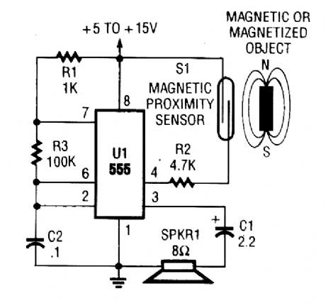
A magnetic need switch enables a 555 osciltator, which drives a speaker. C2 can be varied for different tone frequencies. (View)
View full Circuit Diagram | Comments | Reading(1802)
ELECTROMAGNETIC_FIELD_SENSOR
Published:2009/6/17 22:05:00 Author:May

A telephone pick-up coil is used as a sensing coil. Any 60-Hz hum picked up by the sensing coil is rectified, amplified, and detected, and then drives a meter. (View)
View full Circuit Diagram | Comments | Reading(2569)
27145_MHz_NBFM_RECEIVER
Published:2009/6/17 22:04:00 Author:May

Using a Motorola MC3363 LSI one-chip FM receiver, the circuit is a dual-conversion FM receiver with a 10.7-MHz IF chain. IC4 provides power to drive a small speaker. (View)
View full Circuit Diagram | Comments | Reading(2588)
ANALOG_FREQUENCY_METER
Published:2009/6/17 22:03:00 Author:May


This 1-kHz linear-scale analog frequency meter circuit uses the 555 as a pulse counter. Frequency is read on M1, (or 1 mA meter) which can be calibrated to read 0 to 1 kHz. (View)
View full Circuit Diagram | Comments | Reading(4143)
LOW_CURRENT_AMMETER
Published:2009/6/17 22:03:00 Author:May

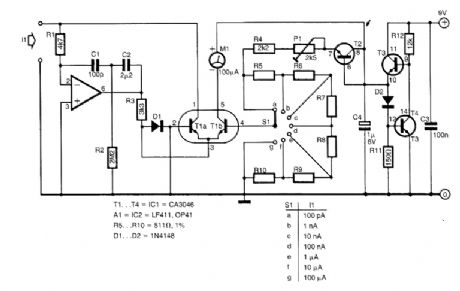
Without using high-value precision resistors, this circuit uses a current mirror, Tla/Tlb. Currents of 100 pA can be measured with this circuit. Ml is a 100-rnA meter. Make sure to use a highquality PC board and low-leakage circuit construction. (View)
View full Circuit Diagram | Comments | Reading(0)
SIMPLE_DIRECT_CONVERSION_RECEIVER_FOR_160_TO_20_M
Published:2009/6/17 22:02:00 Author:May

Note that T1 and T2 are TOKO, including part numbers for the coils T1 and T2. The direct-con-version receiver shown uses a double-tuned input network made from readily available TOKO coils. IC1, an NE602, acts as a VFO and mixer, with the output being an IF frequency in the audio range. IC2 is an audio amplifier, R4 is a volume control. (View)
View full Circuit Diagram | Comments | Reading(3145)
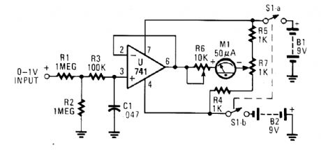
TRANSISTOR_CHECKER
Published:2009/6/17 22:01:00 Author:May


The circuit is built around a 741 general-purpose op amp that is configured as a voltage follower; with the components shown, the op amp has a voltage gain of one. The output of the 741 is used to drive a 50-pA meter rnovement. Potentiometer R7 is used to zero the meter and R6 sets the meter's full-scale reading.
Calibrating the meter is a snap. With no input applied to the circuit, set R6 to mid-position and adjust R7 to zero the meter. Once that is done, apply a positive 1-Vdc voltage to the input and adjust R6 for a full-scale reading. The voltmeter can be adjusted to read both positive and negative voltages by adjusting R7 for a center scale reading at the meter's zero position and a positive 1-V reading at the meter's full-scale position. (View)
View full Circuit Diagram | Comments | Reading(1259)
ONE_IC_CAPACITANCE_TESTER
Published:2009/6/17 22:01:00 Author:May
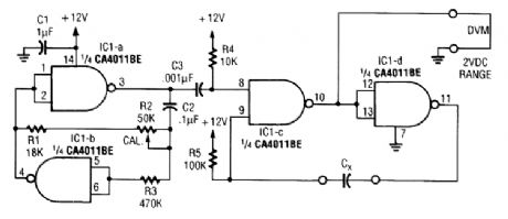
This circuit can be used to match capacitors, etc. The dc output voltage is related to the capacitance values of Cx The circuit values shown are for capacitors in the 0.01-μF order of magnitude, but they can be changed for lower or higher values. (View)
View full Circuit Diagram | Comments | Reading(761)
PULSE_GENERATOR_WITH_VARIABLE_DUTY_CYCLE
Published:2009/6/17 21:59:00 Author:May
Using only one IC and six passive components, this pulse generator has a frequency range of 400 to 4000 Hz and an adjustable duty cycle of 1 to 99%. A threshold detector (ICA) and an in-tegrator (ICB) generate a triangular waveform. A positive voltage at the output of ICA causes the output of ICB to become a negative-going ramp. When the output of this ramp reaches a certain value, ICA, by virtue of its positive-feedback net-work, changes state; its output becomes nega-tive, and the integrator generates positive ramp.This process continually repeats. A voltage fol-lower (ICC) and a 100-kO potentiometer provide a variable ±18-V reference voltage. This reference voltage, along with the triangular waveform, feeds into the positive and negative inputs, respectively, of comparator ICD. You can set the comparator's trip voltage at any point on the triangular waveform; ICD's output changes at that point. Varying the reference voltage alters the duty cycle of the comparator's output by adjusting the potentiometer at the negative input of the integrator, thereby varying the integration time without altering the duty cycle. (View)
View full Circuit Diagram | Comments | Reading(2075)
AUDIO_FREQUENCY_METER
Published:2009/6/17 21:59:00 Author:May

This meter differs from the norm in that it does not use a D'Arsonval movement or digital display to give a reading of the input frequency. Instead, the measured frequency is read from a hand-cali-brated dial.
Any audio signal applied to the circuit is amplified by UI and the resulting output is divided along two paths. In one path, the output signal is applied to the miter; in the other path, the signal is ap-plied to the input of U2 through S1 (a normally open pushbutton switch).
The portion of the amplifier signal that is fed to the mixer is applied to the base of Q1, causing it to toggle on and off at the signal frequency. In the other path, when S1 is pressed, a portion of the op amp's output is applied to U2. If the signal is within the range of U2's internal oscillator's operating frequency, LED1 lights, and a signal is fed to the base of Q2. If the two signals arriving at the mixer do not match exactly, LED2 and LED3 light. That means that the circuit must be fine tuned, which is accomplished by releasing S1 and fine tuning RIB until LED2 and LED3 go out. The dial setting at that point gives the frequency of the input signal to within 1 Hz (or as close as the calibrated dial will allow). (View)
View full Circuit Diagram | Comments | Reading(1452)
ac_WATTS_CALCULATOR
Published:2009/6/17 21:55:00 Author:May
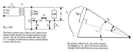
The method basically consists of determining the power factor of the load-the cosine of the phase angle between the voltage across the load and the load circuit. Using a simple circuit, that an-gle can be calculated quite simply.This circuit uses a 1:1 isolation transformer to prevent direct contact with the line. It is wise to proceed with caution whenever voltages of this magnitude are utilized in a test setup, even though the voltages that will be measured are usually below 1 V.RS is a circuit-sense resistor and Rr is a multi-turn potentiometer. The voltage across Rr is ap-proximately 0.5% of the line voltage, which should be sufficient for most applications.Rr is adjusted so that |Vr|=|Vs|; then Vd is measured. In the vector diagram according to Kirchhoff's voltage law, Vs,Vd, and Vr form a triangle, which becomes isosceles by adjusting Rr. Vs is in phase with the load current and Vr is essentially in phase with the load voltage.The power delivered to the load can be calculated as follows: (View)
View full Circuit Diagram | Comments | Reading(722)
50_MHz_RF_BRIDGE
Published:2009/6/17 21:51:00 Author:May
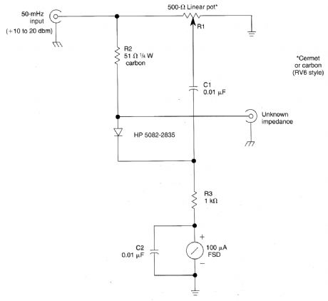
The bridge shown was used for rtteasurements on 50-MHz amateur radio antennas. R1 is a miniature 500Ω linear potentiometer. The unknown impedance is compared to R2, a 51-Ω resistor. An external signal source is required. (View)
View full Circuit Diagram | Comments | Reading(643)
MERCURY_SWITCH_TILT_DETECTOR
Published:2009/6/17 21:50:00 Author:May
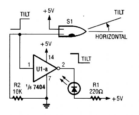
If the mercury bulb in this circuit is tipped,U1-a will light LED1 by going low, indicating a“tilted”condition. (View)
View full Circuit Diagram | Comments | Reading(835)
LIGHT_METER
Published:2009/6/17 21:49:00 Author:May
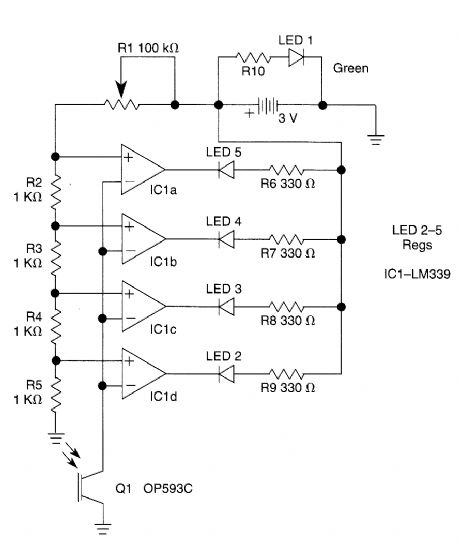
The outputs from the comparators will swing, in sequence, from high to low as the input voltage rises above the reference voltage applied to each comparator. The output LEDs will then switch on in sequence as the voltage rises.The inverting inputs of the comparators are connected in common to the collector of photo-transistor Q1. When Q1 is illuminated, its collec-tor-emitter junction conducts, thereby placing all the inverting inputs within a few millivolts of ground. For most settings of RI, each of the four reference voltages exceeds the value. Therefore, when Q1 is illuminated, the output from each comparator is high and its respective indicator LED is off. (View)
View full Circuit Diagram | Comments | Reading(993)
LOW_DRIFT_dc_VOLTMETER
Published:2009/6/17 21:47:00 Author:May
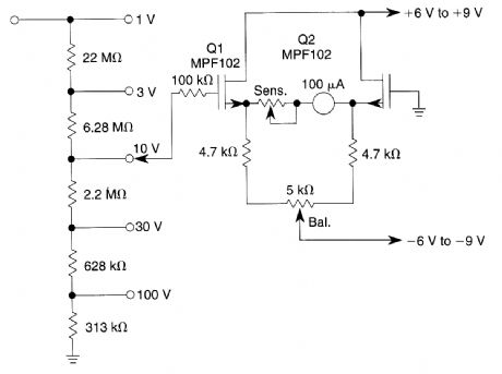
This voltrneter uses a pair of JFETs in a balanced-bridge source-follower amplifier circuit. Q1 and Q2 should be matched within 10% for IDSS This minimizes meter drift and maintains bridge balance over temperature.
(View)
View full Circuit Diagram | Comments | Reading(737)
DELAYED_PULSE_GENERATOR
Published:2009/6/17 21:47:00 Author:May


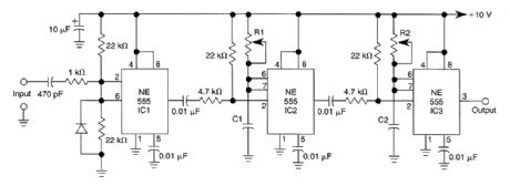
Three 555 IC timers are used in this circuit to construct a simple delayed-pulse generator. IC1 acts as a waveform shaper to produce a rectangular waveform. IC2 produces a delaying pulse to trig-ger IC3 on the trailing edge of the delaying pulse. R1 controls delay time and R2 controls pulse width. As much as a 10:1 range can be generated.Delay: C1= 1.1 x 10⁻⁵ T delay c μFPulse: C2 = 1.1 x 10⁻⁵ T pulse T μsec (View)
View full Circuit Diagram | Comments | Reading(5)
VOLTAGE_LEVEL_CIRCUIT
Published:2009/6/17 21:47:00 Author:May

A DC op amp and a comparator with a ladder reference divider allow a dc input voltage to light one or more LEDs, depending on voltage levels. (View)
View full Circuit Diagram | Comments | Reading(1016)
DIGITALLY_CONTROLLED_SAWTOOTH_PULSE_GENERATOR
Published:2009/6/17 21:29:00 Author:May
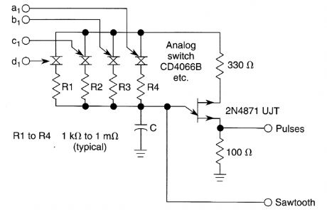
Use of an analog switch as shown allows digital control of a UJT oscillator. (View)
View full Circuit Diagram | Comments | Reading(589)
| Pages:1429/2234 At 2014211422142314241425142614271428142914301431143214331434143514361437143814391440Under 20 |
Circuit Categories
power supply circuit
Amplifier Circuit
Basic Circuit
LED and Light Circuit
Sensor Circuit
Signal Processing
Electrical Equipment Circuit
Control Circuit
Remote Control Circuit
A/D-D/A Converter Circuit
Audio Circuit
Measuring and Test Circuit
Communication Circuit
Computer-Related Circuit
555 Circuit
Automotive Circuit
Repairing Circuit