
Circuit Diagram
Index 1270
The low-power timing switch circuit
Published:2011/7/21 2:06:00 Author:Seven | Keyword: low-power, timing switch
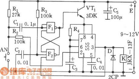
See as the figure, the timing circuit can reduce the 555 static current to l~2μA as it is fixed with the electric switch composed of F1, F2 and VT1. When the power supply is on, as the voltage on C2 can't mutate, so the F2 gate circuit is in a high LEV, the F1 output is located at a low LEV, VT1 is blocked, which makes the static current of the circuit low. When the timing switch AN is pressed, there is a negative pulse on the input terminal of F1, F1 outputs a high LEV, VT is conducting, then 555 has got a power supply voltage.
(View)
View full Circuit Diagram | Comments | Reading(568)
Tuning_fork_stabilized_frequency_standard
Published:2009/7/25 3:46:00 Author:Jessie

This circuit provides both sine and TTL outputs, operates from 5V with low power consumption. Figure 5-26B shows typical waveforms.Trace C is the output of a distortion analyzer connected to the sine output (with has less than 1% distortion, and will drive an 8-Ω load). (View)
View full Circuit Diagram | Comments | Reading(617)
RF_OUTPUT_INDICATOR
Published:2009/6/28 22:32:00 Author:May

Designed for use with amateur radio transmitters Pot is adjusted for maximum desired indication on band usedFor 20-10 meters、6-pF capacitoris adequateOn lower bands (80-40 meters), use 7 or 12 pF instead.-Novice Q & A 73 Magazine, Holiday issue 1976, p 20. (View)
View full Circuit Diagram | Comments | Reading(1732)
The sound control relay circuit
Published:2011/7/23 22:16:00 Author:Seven | Keyword: sound control relay
See as the figure, the circuit consists of the sound detection circuit and single steady trigger circuit, the relay is the executing component. VT1 finish the magnifying job of the input audio signal, when signals come, the 555 is reset, K is pulling in, VT2 is conducting, the electricity on C2 is released by the discharging tube and VT2 in 555. After the sound is gone, both VT1 and VT2 are blocked, C2 charges them through R2 and RP2, the contemporary stable time of the single stable circuit is td =1.1(R2+RP2)C2, the delaying time is 0.05~0.5S which can be adjusted by RP2. (View)
View full Circuit Diagram | Comments | Reading(768)
Portable_oscilloscope_calibrator
Published:2009/7/25 3:46:00 Author:Jessie

This circuit allows a quick check of oscilloscope time-base and vertical calibration. The circuit can be built into a small hand-held box and powered by a 12.5-V battery, as shown. The 30-kΩ resistor should be trimmed for a precise (15 Hz) 1-kHz output using a frequency counter. Accuracy of the 0.1-V, 1-V, and 5-V outputs depends on adjustment of the 2-kΩ pot, and the precision of the fixed resistors. (View)
View full Circuit Diagram | Comments | Reading(1202)
74 Series digital circuit of 74LS256, 74F256 dual 4-bit addressable latch
Published:2011/8/1 4:32:00 Author:Lucas | Keyword: 74 Series , digital circuit , dual 4-bit , addressable latch

d = The H ot L data E before the conversion from low to high; q = the output state in the recent addressing or clearing cycle.
(View)
View full Circuit Diagram | Comments | Reading(710)
RADIATED_FIELD_METER
Published:2009/6/28 22:31:00 Author:May
Gives quick check of overall transmitter performance, including antenna system. Meter can be 1 mA, but 0-200μA or 0-50μA will be more sensitive. The longer the reference antenna used, the greater will be the sensitivity of the meter. Keep lead lengths short. If measurements for various transmitter inputs are recorded when transmitter is work-hg properly, they can serve as guide for later troubleshooting.-E. Hartz, Is My Rig Working or Not?, 73Magazine, Oct. 1976, p 56-57. (View)
View full Circuit Diagram | Comments | Reading(625)
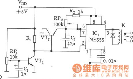
The industrial time relay circuit
Published:2011/7/21 1:51:00 Author:Seven | Keyword: time relay circuit
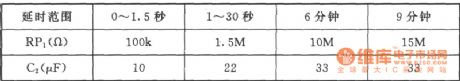
See as the figure, the time relay is to replace JSK, which is designed for the transistor time relay. The circuit includes the step-down regulated voltage source(+12V), 555 single stable circuit and relay control, etc. 555, RP1 and C2 compose the single stable delay circuit, the time td =l.1RP1C2. When the power supply is on, as the 2-pin is in a low LEV, the 555 is reset, K2 is still, when C2 is charged to 2/3VDD by RP1, 3-pin is in a low LEV, K2 is pulling in, which connects with the contactors of K2-1 and K2-2.
(View)
View full Circuit Diagram | Comments | Reading(485)
SIMPLE_CROWBAR
Published:2009/6/28 22:31:00 Author:May

These circuits provide o,vervoltage protection in case of voltage regulator failure or application of an external voltage. Intended to be used with a supply offering some form of short circuit protection, either foldback, current limiting, or a simple fuse. The most likely application is a 5 V logic supply, since TTL is easily damaged by excess voltage. The values chosen in A are for a 5 V supply, although any supply up to about 25 V can be protected by simply choosing the appropriate zener diode. When the supply voltage exceeds the zener voltage +0.7 V, the transistor turns on and fires the thyristor. This shorts out the supply, and prevents the voltage rising any further. In the case of a supply with only fuse protection, it is better to connect the thyristor the regulator circuit when the crowbar operates. The thyristor should have a current rating about twice the expected short circuit current and a maximum voltage greater than the supply voltage. The circuit can be reset by either switching off the supply, or by breaking the thyristor circuit with a switch. (View)
View full Circuit Diagram | Comments | Reading(3250)
74 Series digital circuit of 74251,74LS251 8-to-1 data selector/driver(tristate)
Published:2011/8/1 4:23:00 Author:Lucas | Keyword: 74 Series, digital circuit , 8-to-1 data selector, driver, tristate

View full Circuit Diagram | Comments | Reading(1536)
HIGH_SPEED_WARNING
Published:2009/6/28 22:31:00 Author:May

Audible alarm tone generator drives waming Ioudspeaker to supplement 2-digit speed display that can be set to trip when vehicle speed exceeds 55-mph legal limit. Engine speed signal is taken from primary of spark coil. Switch in transmission activates circuit only when car is in high gear. All functions are performed by sections of LM2900 quad Norton opamp. A1 amplifies and regulates sparlocoil signal. A2 converts signal frequency to voltage proportional to engine speed. A3 compares speed voltage with reference voltage and turns on output transistor at set speed. A4 generates audible tone. Circuit components must be adjusted for number of cylinders, gear and axle ratios, tire size, etc. 10-μF capacitor connectea to A3 can be increased to prevent triggering of alarm when increasing speed mo-mentarily while passing another car.- Linear Applications, Vol. 2, National Semiconductor, Santa Clara, CA 1976, LB-33. (View)
View full Circuit Diagram | Comments | Reading(704)
74 Series digital circuit of 74LS253,74S253 dual 4 to 1 data selector (tristate)
Published:2011/8/1 1:38:00 Author:Lucas | Keyword: 74 Series , digital circuit , dual data selector, 4 to 1, tristate
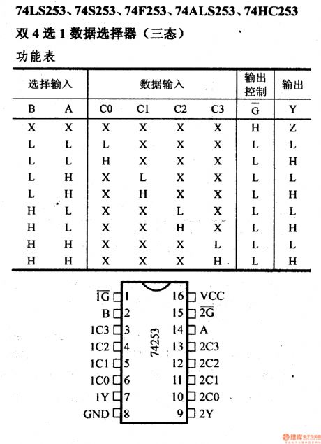
View full Circuit Diagram | Comments | Reading(785)
The D/A converter dual phase complementary frequency generator circuit
Published:2011/7/23 22:29:00 Author:Seven | Keyword: D/A converter, frequency generator
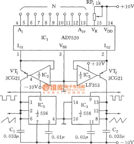
See as the figure, AD7520 is a CMOS 10-bit multi-channel DAC integrated circuit, which can provide with the output current Io1 in forward proportion to the digital input N, it can also provide with the current Io2 in proportion to the (1023-N). Both VT1 and VT2 with wide band dual op-amp LF353 provide with charge current for the capacitors of C1 and C2. When the charge current on C1 and C2 reaches threshold value LEV 2/3VDD, 556 is reset; C1 and C2 are both discharged by the discharging tube in the base plate, and its LEV is reduced to 1/3VDD.
(View)
View full Circuit Diagram | Comments | Reading(627)
LOOP_PREAMP
Published:2009/6/28 22:31:00 Author:May

Loop for lower-frequency amateur bands is connected to gate of HEP802 FET and output to receiver istaken from FET source.C1 is two-gang variable capacitor from old broadcast radio, with stators in parallel to give 600 pF. Article gives loopdata for 40, 80, and 160 meters and for high end of broadcast band. For 40 and 80 meters, use 18-inch square loop with 2 tums spaced 1/4 inch. Ground lower end of 100K resistor to provide ground retum for FET.-K. Comell, Loop Antenna Receiving Aid, Ham Radio, May 1975, p 66-70. (View)
View full Circuit Diagram | Comments | Reading(934)
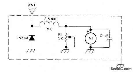
RF_NOISE_BRIDGE
Published:2009/6/28 22:30:00 Author:May

Improves accuracy and measurement range for impedance measurements from 3.5 to 30 MHz, particularly resistive and reactive components of high-frequency antennas. Accuracy is 3 ohms BMS. Wideband noise, generated in zener followed by threetransistor amplifier, is iniected into two legs of bridge in equal amounts by toroidal transformer having quadrifilar windings. With un known impedance connected and detectorlany communication receiver) set to desired frequency, reference impedances (250-ohm noninductive pot and 360-pF variable capacitor) are adjusted for deepest possible null. Value of unknown impedance is then equal to parallel combination of references. Article covers construction and calibration.-R. A. Hubbs and A. F.Doting, Improvements to the nx Noise Bridge, Ham Radio, Feb. 1977, p 10-20. (View)
View full Circuit Diagram | Comments | Reading(3945)
IC_VCO_with_alternate_frequency_sweep_operation
Published:2009/7/25 4:10:00 Author:Jessie

This circuit is an alternate to that of Fig. 5-50, but operates only with negative values of VC. If VC goes to 0 or above, pin 7 is deactivated, and frequency is fixed at 1/(R3C). (View)
View full Circuit Diagram | Comments | Reading(582)
IC_VCO_with_frequency_sweep_operation
Published:2009/7/25 4:09:00 Author:Jessie

This circuit is similar to that of Fig. 5-36, except that the triangle and square outputs are controlled by a sweep or FM input. The frequency is determined by C, R3, RC, VC, and V- as shown by the equations. (View)
View full Circuit Diagram | Comments | Reading(533)
POWER_PROTECTION_CIRCUIT
Published:2009/6/28 22:30:00 Author:May

To safeguard portable, emergency power repeaters from reverse or excessive voltage, D1 prevents incorrect polarity damage, and zener voltage determines the maximum voltage that will reach the rest of the circuitry.Use fast blowing fuse rated greater than the SCR current rating. (View)
View full Circuit Diagram | Comments | Reading(608)
_5_V_from__5_V_or_five_to_eight_cells
Published:2009/7/25 4:09:00 Author:Jessie

Figure 8-116 shows a MAX739 PWM regulator connected to provide -5 V from a five- to eight-cell battery (or a fixed +5-V source). Figure 8-117 shows the efficiency curves. The input voltage range is 3.8 V to 11 V, with a no-load start-up of 4 V maximum, a quiescent current of 1.8 mA (VIN = 5 V), a maximum load current of 200 mA (VIN =5 V), and a 1-μA shutdown current. MAXIM BATTERY MANAGEMENT CIRCUIT COLLECTION, 1994, P. 57. (View)
View full Circuit Diagram | Comments | Reading(497)
IC_VCO_with_single_supply_and_fixed_frequency
Published:2009/7/25 4:07:00 Author:Jessie

This circuit is similar to that of Fig. 5-36, except that a single supply is used, and the output is at a fixed frequency, determined by R3 and C, as shown by the equations. (View)
View full Circuit Diagram | Comments | Reading(591)
| Pages:1270/2234 At 2012611262126312641265126612671268126912701271127212731274127512761277127812791280Under 20 |
Circuit Categories
power supply circuit
Amplifier Circuit
Basic Circuit
LED and Light Circuit
Sensor Circuit
Signal Processing
Electrical Equipment Circuit
Control Circuit
Remote Control Circuit
A/D-D/A Converter Circuit
Audio Circuit
Measuring and Test Circuit
Communication Circuit
Computer-Related Circuit
555 Circuit
Automotive Circuit
Repairing Circuit