Amplifier Circuit
The low-power timing switch circuit
Published:2011/7/21 2:06:00 Author:Seven | Keyword: low-power, timing switch | From:SeekIC

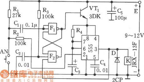
See as the figure, the timing circuit can reduce the 555 static current to l~2μA as it is fixed with the electric switch composed of F1, F2 and VT1. When the power supply is on, as the voltage on C2 can't mutate, so the F2 gate circuit is in a high LEV, the F1 output is located at a low LEV, VT1 is blocked, which makes the static current of the circuit low. When the timing switch AN is pressed, there is a negative pulse on the input terminal of F1, F1 outputs a high LEV, VT is conducting, then 555 has got a power supply voltage.
Reprinted Url Of This Article:
http://www.seekic.com/circuit_diagram/Amplifier_Circuit/The_low_power_timing_switch_circuit.html
Print this Page | Comments | Reading(3)

Article Categories
power supply circuit
Amplifier Circuit
Basic Circuit
LED and Light Circuit
Sensor Circuit
Signal Processing
Electrical Equipment Circuit
Control Circuit
Remote Control Circuit
A/D-D/A Converter Circuit
Audio Circuit
Measuring and Test Circuit
Communication Circuit
Computer-Related Circuit
555 Circuit
Automotive Circuit
Repairing Circuit
Code: