
Circuit Diagram
Index 1274
74 Series digital circuit of 74195,74LS195A 4-bit parallel access shift register
Published:2011/8/1 0:56:00 Author:Lucas | Keyword: 74 Series, digital circuit , 4-bit parallel access , shift register

The typical maximum clock frequency of 74195,74 LS195A is 39MHz, and 74S195 is 105MHz; the typical operating frequency of 74HC195 is 45Hz.
a, b, c, d = the corresponding steady input level of A, B, C, D. QA0, QB0, QC0, QD0= the corresponding level of QA, QB, QC, QD before the establishment of steady-state input conditions. QAn, QBn, QCn= the corresponding level of QA, QB, QC at the latest time hopping.
(View)
View full Circuit Diagram | Comments | Reading(3424)
REGULATED_VOLTAGE_DIVIDER
Published:2009/6/28 22:01:00 Author:May

ICs requiring 3.6 or 6 volts can be run from a battery or fixed regulated supply of a higher voltage by using the circuit shown. The transistor should be mounted on a heatsink as considerable power will be dissipated by its collector.Additional filtering can be obtained by fitting a capacitor (C1) as shown. The capacitance is effectively multiplied by the gain of the transistor. A ripple of 200 mV (peak to peak) at the input can be reduced to 2 mV in this fashion. Maximum output current depends on the supply rating and transistor type (with heatsink) used. (View)
View full Circuit Diagram | Comments | Reading(1063)
RE_PROBE_FOR_VTVM
Published:2009/6/28 21:58:00 Author:May

This circuit combines a 555 timer with a 2N2222 transistor and an extemal potentiometer. The pot adjusts the output voltage to the desired value. To regulate the output voltage, the 2N2222 varies the control voltage of the 555 IC, increasing or decreasing the pulse repetition rate. A 1.2 K resistor is used as a collector load. The transistor base is driven from the extemal pot. If the output voltage becomes less negative, the control voltage moves closer to ground, causing the repetition rate of the 555 to increase, which, in turn, causes the 3 μF capacitor to charge more frequently. Output voltage for the circuit is 0 to 10 V, adjusted by the extemal pot. Output regulation is less than five percent for 0 to 10 mA and less than .05 percent for 0 to 0.2 mA. (View)
View full Circuit Diagram | Comments | Reading(606)
The 3-terminal stabilizer switch regulator power supply circuit
Published:2011/7/24 3:41:00 Author:Seven | Keyword: 3-terminal stabilizer, switch regulator


The switch regulator power supply circuit formed by the 3-terminal stabilizer can be understood by the equivalent circuit. As some reasons, the output voltage falls down slightly, the distributed voltage V3 on R5 and R6 is also falls down, after being amplified by VT3, IC3 decreases, i.e the current past R1 and VD1 is falling down, which leads to the drop of V1 and rise of IC1, V4 is rising up after being distributed by R2 and R3, V2 is rising up with it, accordingly, V3 falls```
(View)
View full Circuit Diagram | Comments | Reading(510)
THREE_AMPLIFIER_NOTCH_FILTER(OR_ELLIPTIC_FILTER_BUILDING_BLOCK)
Published:2009/6/28 21:58:00 Author:May


View full Circuit Diagram | Comments | Reading(582)
ADJUSTABLE_OUTPUT_REGULATOR
Published:2009/6/28 21:57:00 Author:May

The addition of an operational amplifier allows adjustment to higher or intermediate values while retaining regulation characteristics; The minimum voltage obtainable with this arrangement is 2.0 volts greater than the regulator voltage. (View)
View full Circuit Diagram | Comments | Reading(665)
POWER_SUPPLY_WITH_ADJUSTABLE_CURRENT_LIMIT_AND_OUTPUT_VOLTAGE
Published:2009/6/28 21:56:00 Author:May

View full Circuit Diagram | Comments | Reading(1312)
74 Series digital circuit of 74194,74LS194A 4-bit two-way general shift register
Published:2011/8/1 0:53:00 Author:Lucas | Keyword: 74 Series , digital circuit , 4-bit two-way , general shift register


The typical maximum clock frequency of 74197,74 LS194A is 36MHz, and 74S194 is 104MHz; the typical operating frequency of 74HC194 is 45Hz.
a, b, c, d = the corresponding steady input level of A, B, C, D. QA0, QB0, QC0, QD0= the corresponding level of QA, QB, QC, QD before the establishment of steady-state input conditions. QAn, QBn, QCn= the corresponding level of QA, QB, QC at the latest time hopping.
(View)
View full Circuit Diagram | Comments | Reading(3083)
DUAL_OUTPUT_BENCH_POWER_SUPPLY
Published:2009/6/28 21:55:00 Author:May

View full Circuit Diagram | Comments | Reading(581)
FREQUENCY_DIVIDER_CHAIN
Published:2009/6/28 21:54:00 Author:May

Circuit NotesSawtooth output from each stage IS one half frequency of preceding stage. (View)
View full Circuit Diagram | Comments | Reading(589)
Simple_Z80_interface
Published:2009/7/25 5:08:00 Author:Jessie
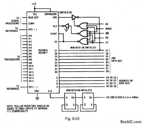
Figure 9-22 shows the ADC0816/17 connected to form a simple interface with classic Z80-type microprocessors. The 280, even though architecturally similar to the INS8080, uses slightly different control lines to perform I/O reads and writes. NOR gates are used to strobe the I/O functions. However, the Z80 has RD (read) and WR (write) strobes, which are gated with IOREQ (I/O request). START is connected to OE. This causes a new conversion to be started whenever the data bits are read. (Such a configuration can be useful if the converter is to be continually restarted upon completion of the previous conversion.) Address bit A6 is used to drive a strobe that placed EOC on the data bus to be read by the CPU. NATIONAL SEM[CONDUCTOR, APPLICATION NOTE 258, 1994, P. 607.
(View)
View full Circuit Diagram | Comments | Reading(1001)
100_V/025_A_SWITCH_MODE_CONVERTER
Published:2009/6/28 21:53:00 Author:May

View full Circuit Diagram | Comments | Reading(563)
8080_interface_with_partial_decoding
Published:2009/7/25 5:06:00 Author:Jessie
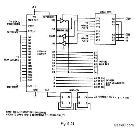
Figure 9-21 shows the ADC0816/17 connected with a DM74LS139 dual 2-4 decoder to form an 8080 interface with partial decoding. One half of the DM74SL139 is used to create read pulses, and the other half to create write pulses. The START and OE inputs are inverted to provide the correct pulse polarity. This interface partially decodes A6 and A7 to provide more I/O capabilities than the Fig. 9-20 circuit. The circuit in Fig. 9-21 also implements a simple polled-I/O structure. The EOC output is placed on the data bus by a tristate inverter when the inverter is enabled by a read pulse from the INS8080.
(View)
View full Circuit Diagram | Comments | Reading(598)
Simple_8080_interface
Published:2009/7/25 5:04:00 Author:Jessie
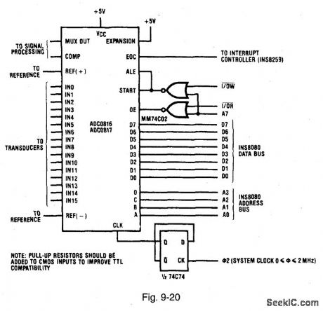
Figure 9-20 shows connections for interface between the ADC0816/17 and classic 8080-type microprocessors (INS8080/8224/8228). This interfacing is quite simple because the INS8080 CPU has separate I/O read (I/OR) and I/O write (I/OW) strobes (or separate I/O addressing). As a result, in this simple interface systems, little or no address decoding is required. Two NOR gates are used to gate the I/O strobes with the most-significant address bit A7. (The INS8080 has 8 bits of port address, yielding a maximum of four I/O ports if inputs A, B, C, and D are connected to the address bus.) An MM74C74 flip-flop is used as a divide-by-2 to generate a converter clock of 1 MHz. If the system clock is equal to or less than 1 MHz, the flip-flop can be omitted, Typical software for the Fig. 9-20 circuit first writes the channel address to the converter as a start signal. The two start pulses are sent to the ADCs to allow the comparator input to settle. After the second start pulse, the CPU can execute other program segments until the CPU is interrupted by EOC going high. Depending on interrupt structure, program control is then given to the interrupt handler, which reads the converter data. NATIONAL SEMICONDUCTOR, APPLICATION NOTE 258, 1994, P. 606. (View)
View full Circuit Diagram | Comments | Reading(1000)
Microprocessor_interface_considerations
Published:2009/7/25 5:02:00 Author:Jessie
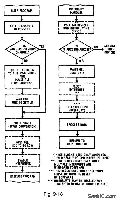
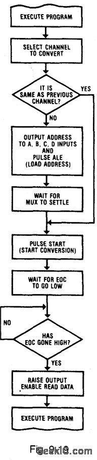
Figures 9-18 and 9-19 show flow charts for the interrupt-control and polled-I/O modes of ADC/microprocessor interface, respectively. Either interface can be used with the ADC0816/17, but the polled-I/O method usually requires fewer external components. With polled-I/O, the microprocessor (or CPU) periodically interrogates the ADC which looks like an I/O port to the CPU. With interrupt-control, the ADC appears as a memory and interrupts the microprocessor. From a simplified-design standpoint, the major concern is whether the EOC (end of conversion, Figi 9-3) should be polled by the microprocessor. Even though the actual timing of CPU read and write cycles varies, most microprocessors output the address and data (during write) onto the system buses. A certain time later, the read or write strobes go active for a specified time. The interface logic must detect the state of the address and data buses and initiate the action. For the ADC0816/17; these actions are: (1) load channel address, (2) start conversion, (3) detect EOC, and (4) read the resultant data. These functions are performed by decoding the read-write strobes, address, and data to form ALE and START pulses, then to detect EOC, and finally to read the data. NATIONAL SEMICONDUCTOR, APPLICATION NOTE 258, 1994, P. 605. (View)
View full Circuit Diagram | Comments | Reading(625)
TACH_DWELL_METER
Published:2009/6/28 21:53:00 Author:May
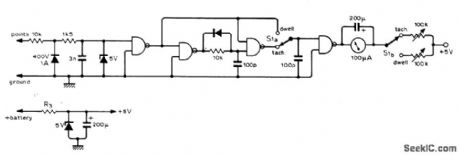
Built around SN7402 NOR-gate IC. Requires no internal battery; required 5 V is obtained by using 50 ohms forR3 in zener circuit shown if car battery is 6 V, and 300 ohms if 12 V. Article gives calibration procedure for engines having 4, 6, and 8 cylinders; select maximum rpm to be indicated, multiply by number of cylinders, then divide by 120 to get frequency in Hz.-N. Parron, Tach-Dwell Meter, Wireless World, Sept. 1975, p 413. (View)
View full Circuit Diagram | Comments | Reading(2227)
ADC_with_sample_rand_hold_S_H
Published:2009/7/25 5:00:00 Author:Jessie
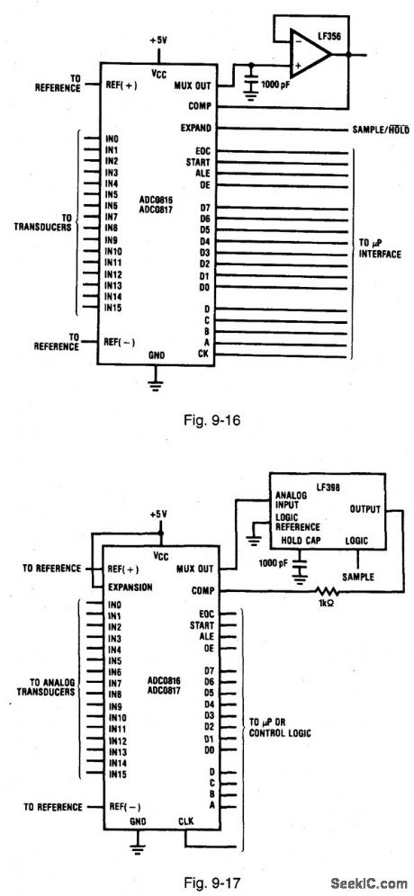
Figures 9116 and 9-17 show the ADC0816/17 connected for S/H operation. (The S/H function is the only major data-acquisition element not included in these ADCs.) If the input signals are fast moving, then an S/H should be used to quickly acquire the signal, then hold the signal while the ADCs convert it to a digital readout. This can be implemented by inserting an S/H function between the multiplexer output and the comparator input. In the simplest form, the multiplexer output is connected to the comparator input, with a capacitor connected to ground (similar to that shown in Fig. 9-16). The expansion-control pin is used as a sample-control input. When EXPAND is high, one switch is on and the capacitor voltage follows the input. When EXPAND is low, all switches are turned off and the capacitor holds the last value. However, this simple solution is not practical. The input bias to the comparator is about 2 μA (worst case, with a clock of 640 kHz). The droop (discharge rate) for a 1000-pF capacitor is about 2000 V/s (about 0.2-V per conversion). This is not practical. If a 0.01-μF capacitor is used instead, the rate is about 20 μV, which might work. However, the acquisition time would be about 100 μs, about the length of a conversion. The circuit of Fig. 9-16 eliminates the problem produced by the high comparator-input leakage. With the LF356 buffer connected between the multiplexer-output and comparator input pins, the leakage is reduced from 2 μA to about 100 nA. The droop-per-conversion is typically less than 1.0 μV per conversion (with the 1000-μF capacitor shown) and the acquisition time is about 20 ps (instead of the 100 ps). The circuit of Fig. 9-16 isolates the capacitor from both the multiplexer and comparator pins using an LF398 IC sample-and-hold. Acquisition time for the LF398 is a typical 4 μs to (0.1%), and droop rate is about 20 μV/conversion. Because the LF398 has its own S/H input, the expansion control of the ADC is free to be used in the normal manner. Use a hold capacitor with minimum dielectric absorption (polypropylene and polystyrene) for best results. NATIONAL SEMICONDUCTOR, APPLICATION NOTE 258, 1994, P. 603, 604. (View)
View full Circuit Diagram | Comments | Reading(641)
74 Series digital circuit of 74192,74L192 preset BCD decimal synchronous reversible counter(dual clock with clear)
Published:2011/8/1 0:45:00 Author:Lucas | Keyword: 74 Series , digital circuit , preset BCD decimal , synchronous reversible counterd, ual clock with clear


View full Circuit Diagram | Comments | Reading(3141)
CMOS_PROGRAMMABLE_DIVIDE_BY_N_COUNTER
Published:2009/6/28 21:53:00 Author:May

Circuit Notes
A single connection change permits division by any integer between 2 and 10. The RCA CD4017A Johnson decade counter is shown connected as a divide by 7 counter. The resistor is used to hold the reset line low. When the appropriate number is reached, that output and the reset line are driven high, resetting the counter. To divide by other integers, pin 15 should be connected to the desired output. For example, pin 1 for a divide by 5, or pin 7 for a divide by 3. The output of the divider appears on the 0 line. (View)
View full Circuit Diagram | Comments | Reading(1360)
ADC_with_at_icroprocessor_con_trolled_gain
Published:2009/7/25 4:58:00 Author:Jessie
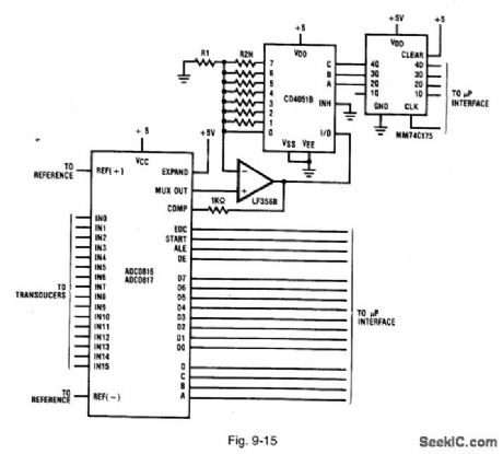
Figure 9-15 shows the ADC0816/17 connected for an external gain-control under supervision of a microprocessor. The CD4051 analog multiplexer is placed in the feedback loop of a simple noninverting op amp. The op-amp gain is controlled by selecting one of the CD4051 analog switches. This cuts a resistor in and out of the feedback loop. If the resistors (R2N) are of different value, different gains are realized. The gains are given by: Gain (AV) = 1 + (R2N/R1). A microprocessor (or some control logic) selects a gain by latching the channel address into a MM74C173. The LF356B output must not exceed the power supply. As a result, the op-amp gain must be reduced to a new level before a new channel is selected. The 1-kΩ resistor at the LF356B output helps protect the comparator inputs from accidental overvoltage (or undervoltage). The two back-biased diodes at the input to VCC and ground (1N914 or Schottky) offer further protection. NATIONAL SEMICONDUCTOR, APPLICATION NOTES 258, 1994, P. 602.
(View)
View full Circuit Diagram | Comments | Reading(845)
| Pages:1274/2234 At 2012611262126312641265126612671268126912701271127212731274127512761277127812791280Under 20 |
Circuit Categories
power supply circuit
Amplifier Circuit
Basic Circuit
LED and Light Circuit
Sensor Circuit
Signal Processing
Electrical Equipment Circuit
Control Circuit
Remote Control Circuit
A/D-D/A Converter Circuit
Audio Circuit
Measuring and Test Circuit
Communication Circuit
Computer-Related Circuit
555 Circuit
Automotive Circuit
Repairing Circuit