
Circuit Diagram
Index 1190
OSCILLATOR_WITH_DOUBLE_FREQUENCY_OUTPUT
Published:2009/7/1 2:36:00 Author:May
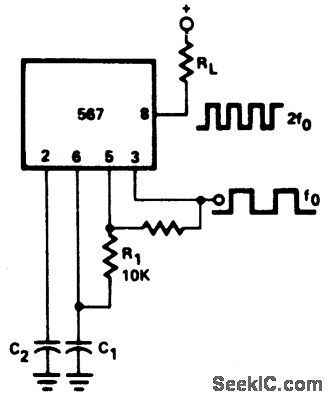
View full Circuit Diagram | Comments | Reading(601)
GATE_TURNOFF_D_C_CIRCUIT_BREAKER
Published:2009/7/24 4:07:00 Author:Jessie

Closing on switch discharges C1 into gate to initiate turn-on. Closing off switch discharges C2 out of pate, opening power circuit.-J. W. Motto, Jr., Switching Circuits Using the Gate Turnoff Controlled Rectifier, EEE, 13:3, p 52-55. (View)
View full Circuit Diagram | Comments | Reading(622)
LOW_FREQUENCY_DOUBLER
Published:2009/7/1 2:34:00 Author:May
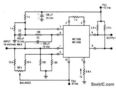
View full Circuit Diagram | Comments | Reading(1379)
Adjustable_step_up_converter
Published:2009/7/24 4:07:00 Author:Jessie


Figure 8-12 shows a MAX757 connected to provide an adjustable output from 2.7 V to 5.5 V, with a low-battery function. Figure 8-13 shows component suppliers. Let R2 be 100 kΩ, and select R1 for a desired output using:Where VREF is 1.25 V. Let R4 100 kΩ, and select R3for a desired threshold of the low-battery detector using:where VREF is 1.25V. MAXIM NEW RELEASES DATA BOOK, 1994. P. 4-178. (View)
View full Circuit Diagram | Comments | Reading(872)
IGNITRON_SHORTS_SPARK_GAP
Published:2009/7/24 4:07:00 Author:Jessie

Used for continuous production of plasma in mirror-geometry magnetic Geld of Philips ionization gage. Ignitron shorts spark gap about 100 microsec aftet discharge begins. Ionization gage (PIG) receives positive potential at peak of externally applied magnetic fold by dosing of triggered spark gap.-M. F. Wolff, Plasma Engineering-Part 1 : Generating and Heating Plasma, Electronics, 34:24, p 47-53. (View)
View full Circuit Diagram | Comments | Reading(1484)
Solid_state_circuit_breaker
Published:2009/7/24 4:18:00 Author:Jessie

This circuit is the solid-state equivalent of a circuit breaker. The circuit turns off the main regulator output within 700 ns of an overload using the values shown. The trip current and breaker-delay point are settable over a wide range. Under normal operation, current through the 1-Ω shunt is insufficient to bias Q1 into conduction. Q2 is also off and the regulator produces an output. When an overload occurs (Trace A of Fig. 9-4B is the regulator output current), the potential across the 1-Ωresistor rises, turning on Q1. This drives the Q2 base (trace B), and turns Q2 on, grounding the enable pin (trace C) to shut down the regulator output (trace D). The 10-kΩ values from the main output to the pin latch the regulator down. The 1-Ω value can be changed to accommodate other desired current-trip points. The 4.7-μ.F capacitor (in dashed lines) can be added (delete the 100-pF capacitor) for applications where fast response is not desired. (View)
View full Circuit Diagram | Comments | Reading(984)
TEMPORARY_MEMORY
Published:2009/7/24 4:17:00 Author:Jessie

Arrangement using Esaki or tunnel diode is equivalent to bistable flip-flop. Used in 24-channel pulse code modulation system.-T. Kojima and M. Watanabe, When You're Second, You Try Harder, Electronics, 38:25, p 81-89. (View)
View full Circuit Diagram | Comments | Reading(657)
SENSITIVE_D_C_POWER_SWITCH
Published:2009/7/24 4:17:00 Author:Jessie

Stays on after being triggered, to give latching action. Power input is 2.5 microwatts, power output is 44,000, and power gain is 92 db.- Transistor Manual, Seventh Edition, General Electric Co., 1964, p 331. (View)
View full Circuit Diagram | Comments | Reading(545)
AUDIO_SWITCH
Published:2009/7/24 4:16:00 Author:Jessie

Switches audio signal on and off under control of flip-flop. With potentiometer across output, phase can be reversed. With two of these switches connected to same flip-flop, and each excited by different audio signal, potentiometer connected between B outputs will provide signal from wiper to ground that alternates from one audio signal to other as flip-flop changes state. Pot setting determines relative amplitudes of two signals. Can be used to generate a-f shift-keying signals.-F. Stevens, Audio On-Off, Phase-Reversing Switch, EEE,14:6, p 91-92. (View)
View full Circuit Diagram | Comments | Reading(878)
Level_detector_for_photodiode
Published:2009/7/24 4:16:00 Author:Jessie

Fig. 15-3 This photodiode level detector operates from a single -10-V supply and is suitable for MOS logic. The output changes state when the D1 current reaches 1μA. Even at this low current, the error contributed by the LM111 is less than 1%. Higher threshold currents can be obtained by reducing R1, R2, and R3 proportionally. At the switching point, the voltage across D1 is nearly zero, so the D1leakage current does not cause an error. The output switches between ground and -10 V, The circuit will operate with a 5-V supply by reducing the values of R1, R2, and R3. Circuit accuracy depends on supply regulation because the reference is derived from the supply. National Semiconductor, Linear Applications Handbook 1991, p. 130. (View)
View full Circuit Diagram | Comments | Reading(764)
HIGH_POWER_SCR_STATIC_SWITCH
Published:2009/7/24 4:16:00 Author:Jessie

Prevents burning of switch or relay contact when switching large inductive loads. Switch contacts here carry only trigger current for silicon controlled rectifiers. If desired, output power can be varied by changing time constant R1-C1 to control scr firing angle. Will switch primary of transformer having 4,200 v-a secondary load.-J. A. Moraites, High Power AC Static Switch, EEE, 12:8, p 71. (View)
View full Circuit Diagram | Comments | Reading(1321)
1_MILLIMICROSEC_SPARK_GAP_SWITCH
Published:2009/7/24 4:15:00 Author:Jessie

Spark gaps are mounted so ultraviolent to diction from gaps that ire earlier in 111-gap operating sequence irradiate succeeding gaps. Intense radiation front earlier gaps reduces statistical firing delay, or jitter, of succeeding gaps. Breakdown of gap is further speeded by connecting low-potential end of gap to trigger source with short length of cable and blocking capacitor, which in turn is grounded by similar cable.-H. B. McFarlane, Spark Gaps for Fast-High Voltage Switching, Electronics, 32:31, p 72-73. (View)
View full Circuit Diagram | Comments | Reading(635)
Zero_crossing_detector_for_magnetic_transducer
Published:2009/7/24 4:14:00 Author:Jessie

Fig, 15-2 This circuit detects zero crossing in the output of a magnetic transducer within a fraction of 1 mV. The resistive divider, R1 and R2, biases the inputs 0.5 V above ground, within the common-mode range of the LM111. The output will drive DTL or TTL directly. Because the output must drive any capacitive loading for positive-going output signals, the value of R5 determines circuit speed (a lower value increases speed). An optional offset-balancing circuit using R3 and R4 is included in the schematic. National Semiconductor Linear Applications Handbook 1991, p 130. (View)
View full Circuit Diagram | Comments | Reading(1753)
SEQUENTIAL_SWITCHING
Published:2009/7/24 4:14:00 Author:Jessie

Shock-resistant design releases number of solenoid-operated mechanical locks at 10-millisec intervals. Single-stroke ramp generator Q1 starts sequence when dosing of initiation switch S1 discharges C1. Q2 reduces loading on timing circuit R1-C1 when large base currents are drawn. Ramp is sufficiently linear to provide adequate timing accuracy for eight operations.-D. H. Thompson and D. Simpson, Time-Sequence Switch, Electronics, 33:28, p 64. (View)
View full Circuit Diagram | Comments | Reading(820)
Basic_comparator
Published:2009/7/24 4:14:00 Author:Jessie
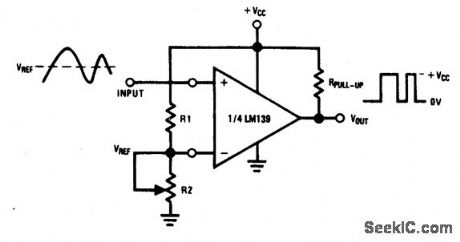
Fig. 15-1 This basic comparator circuit converts low-level analog signals to a high-level digital output. The pull-up resistor value should be high enough to avoid excessive power dissipation, yet low enough to supply sufficient drive to switch the load current at the comparator output. Resistors R1 and R2 set the input threshold trip voltage (VREF) at any value within the input common-mode range of the comparator. Notice that comparator common-mode characteristics are essentially the same as for op amps described in chapter 10. For example, with a VCC of 10 V, and both R1 and R2 at 5 kΩ, VREF can be set to any value up to 5V. National Semiconductor. Linear Applications Handbook, 1991, p. 257 (View)
View full Circuit Diagram | Comments | Reading(1860)
LIGHT_BEAM_COUPLING
Published:2009/7/24 4:14:00 Author:Jessie

Gallium arsenide light source and silicon photodetector prevent interaction between drive circuit and output of binary switch.-E. L. Bonin, Light-Coupled Semiconductor Switch for Low-Level Multiplexing, Electronics, 38:3, p 54-59. (View)
View full Circuit Diagram | Comments | Reading(499)
SIMPLE_DIGITAL_PANEL_METER_POWER_SOURCE
Published:2009/7/24 4:22:00 Author:Jessie

This source will supply 9 to 12 Vdc with floating ground, needed by many digital panel meters. (View)
View full Circuit Diagram | Comments | Reading(825)
Comparator_for_ground_referred_load
Published:2009/7/24 4:22:00 Author:Jessie
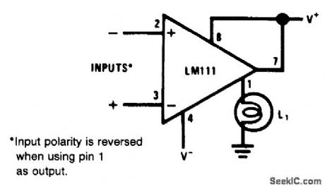
Fig. 15-8 This circuit uses a comparator to drive a ground-referred load, and it is useful during switching operations. An incandescent lamp draws a high inrush current when power is first applied (cold-filament resistance is typically 8 times slower than when the filament is heated). The high inrush current can damage a switch. The current limiting of the LM111 holds the inrush current to a safe level. Note that input polarity is reversed because the ground terminal of the LM111 is used as the output. National Semiconductor Linear Applications Handbook 1991, p. 1204. (View)
View full Circuit Diagram | Comments | Reading(583)
SOLID_STATE_DPDT_SWITCH
Published:2009/7/24 4:22:00 Author:Jessie

Eight diodes and four transistors connected as shown give same action as double-pole double-throw relay.-R. C. Going, Solid-State DPDT Relay, EEE, 11:10, p 26-27. (View)
View full Circuit Diagram | Comments | Reading(1908)
Zero_crossing_detector_for_MOS
Published:2009/7/24 4:21:00 Author:Jessie
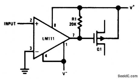
Fig. 15-7 In this zero-crossing detector, the ground terminal of the LM111 is connected to V-. With±15-V supplies, the signal swing delivered to the gate of Q1 is also ±15 V, so the circuit is well suited for MOS (particularly where the gain or feedback of a circuit must be changed at some precisely determined signal level). The circuit can be modified to work with JFETs. National semiconductor Linear Applications Handbook 1991, p 1204.
(View)
View full Circuit Diagram | Comments | Reading(690)
| Pages:1190/2234 At 2011811182118311841185118611871188118911901191119211931194119511961197119811991200Under 20 |
Circuit Categories
power supply circuit
Amplifier Circuit
Basic Circuit
LED and Light Circuit
Sensor Circuit
Signal Processing
Electrical Equipment Circuit
Control Circuit
Remote Control Circuit
A/D-D/A Converter Circuit
Audio Circuit
Measuring and Test Circuit
Communication Circuit
Computer-Related Circuit
555 Circuit
Automotive Circuit
Repairing Circuit