
Index 139
Linear_current_regulator
Published:2009/7/23 23:06:00 Author:Jessie
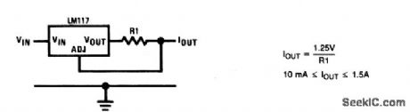
This circuit provides regulated current from 10mA to 1.5A, depending on the value of R1. (View)
View full Circuit Diagram | Comments | Reading(668)
Positive_and_negative_voltage_converter
Published:2009/7/23 23:05:00 Author:Jessie
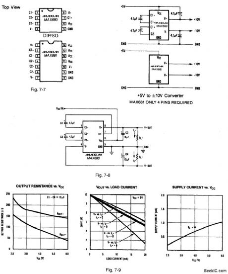
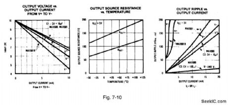
Figure 7-7 shows MAX680 and MAX681 converters used to provide ±10-V outputs from a +5-V input. The input voltage range is +2.0 V to +6.0 V. Voltage-conversion efficiency is 95%, with 85% power-conversion efficiency. The supply current is 500 μA. The output source impedances are typically 150 Ω, providing useful output currents up to 10 mA. No extemal capacitors are required for the MAX681. Figure 7-8 shows a test circuit. Figures 7-9 and 7-10 show typical test results. MAxIM NEw RELEASES DATA BOOK, 1992, P. 4-141. (View)
View full Circuit Diagram | Comments | Reading(726)
Linear_regulator_with_multiple_outputs
Published:2009/7/23 23:05:00 Author:Jessie
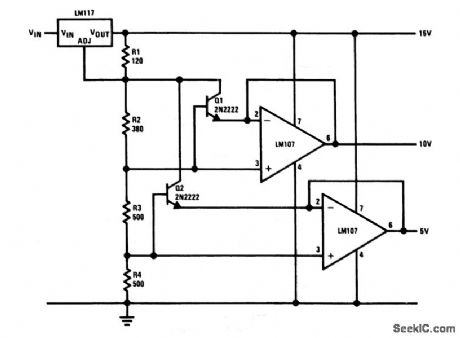
This circuit provides +5-, +10-, and +15-V regulated outputs. (View)
View full Circuit Diagram | Comments | Reading(530)
Linear_voltage_regulator_and_voltage_reference
Published:2009/7/23 23:04:00 Author:Jessie

This circuit provides a +15-V regulated output, as well as a 6.95-V voltage reference. (View)
View full Circuit Diagram | Comments | Reading(576)
Adjustable_regulator_with_protective_diodes
Published:2009/7/23 23:10:00 Author:Jessie
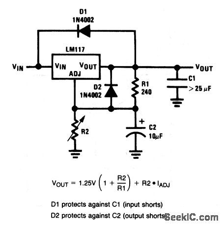
This circuit is similar to that of Fig. 7-11, but with diodes that protect against capacitor discharge (because of input or output shorts). (View)
View full Circuit Diagram | Comments | Reading(634)
Adjustable_regulator_with_improved_ripple_rejection
Published:2009/7/23 23:09:00 Author:Jessie
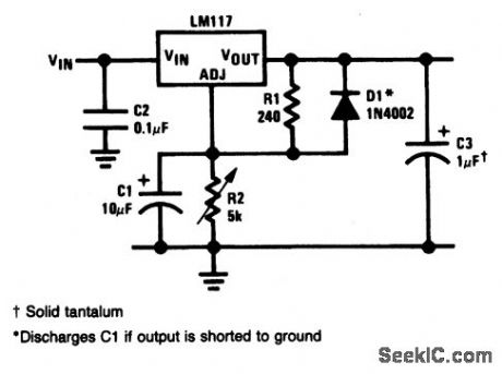
This circuit is similar to that of Fig. 7-11, but with improved ripple rejection. (View)
View full Circuit Diagram | Comments | Reading(633)
Charge_pump_F_V_converter
Published:2009/7/23 23:09:00 Author:Jessie
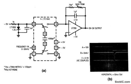
Pig. 12-1 In this circuit, the frequency input is applied to the clock input of an LTC1043 switched-capacitor IC. The 1000-pF capacitor is switched between a fixed voltage and the inverting input of the LF356. The 1-pF feedback capacitor averages this action over several cycles, and the circuit output is a dc level that is linearly related to frequency. The feedback resistors set the LF356 gain. Note that the input pulse width must be low for at least 100 ns to allow complete discharge of the 1000-pF capacitor. To trim, apply 30-kHz to pin 16 of the LTC1043 and set the gain trim for exactly 3.0V. Linear Technology Linear Applications Handbook 1990p.AN3-11. (View)
View full Circuit Diagram | Comments | Reading(616)
Two_wire_current_transmitter
Published:2009/7/23 23:09:00 Author:Jessie
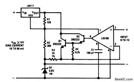
This circuit has a 10- to 50-mA output for a 1-V input. The minimum operating voltage is about 12 V. The circuit can be used in 4- to 20-mA current-transmitter applications (industrial control). However, the LM117 should be selected for low quiescent current. (View)
View full Circuit Diagram | Comments | Reading(600)
Adjustable_linear_current_regulator
Published:2009/7/23 23:08:00 Author:Jessie
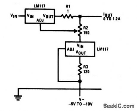
This circuit provides regulated current from 0 to 1.2A, as set by R2. (View)
View full Circuit Diagram | Comments | Reading(630)
Adjustable_constant_voltage_constant_current_regulator
Published:2009/7/23 23:07:00 Author:Jessie
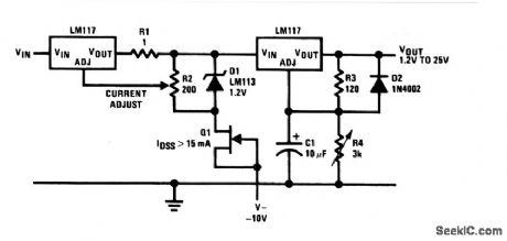
This circuit has a 1.2- to 15-V output range, set by R4. Current remains constant between 0 and 1.2 A, set by R2. (View)
View full Circuit Diagram | Comments | Reading(1285)
Multiple_on_card_regulators_with_single_control
Published:2009/7/23 23:13:00 Author:Jessie
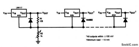

This circuit shows a method of adjusting several on-card regulators with a single control. All outputs should track within t 100 mV, with a minimum 10-mA load. (View)
View full Circuit Diagram | Comments | Reading(563)
5_V_logic_regulator_with_electronic_shutdown
Published:2009/7/23 23:12:00 Author:Jessie
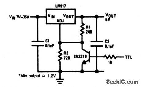
This circuit is suitable for 5-V logic applications and can be shut down electronically with a TTL-level signal. (View)
View full Circuit Diagram | Comments | Reading(705)
General_purpose_linear_supply_regulator
Published:2009/7/23 23:11:00 Author:Jessie
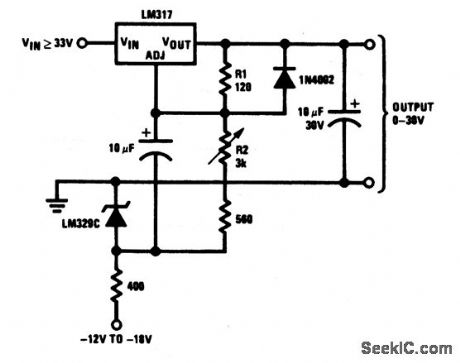
This circuit can be used as a general-purpose lab supply. Although a negative source must be provided, the source does not need to be well regulated. (View)
View full Circuit Diagram | Comments | Reading(563)
F_V_converter_with_sample_hold_and_active_filter
Published:2009/7/23 23:54:00 Author:Jessie
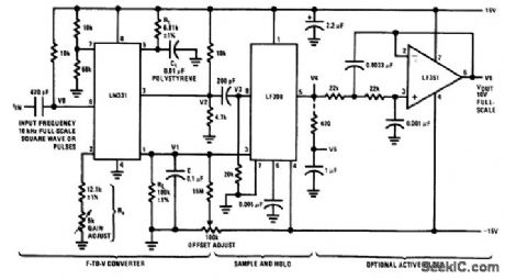
Fig, 12-20 This circuit uses both a sample/hold and an active filter to minimize the ripple/response tradeoff. With the values shown, ripple (at V6) is about 1 mVp-p. Response or settling time to a step change of input frequency is about 60 ms. Linearity is better than 0.1% from 10 kHz down to 500 Hz, but becomes increasingly nonlinear below 500 Hz. To trim, apply 1 kHz and set the offset adjust for 1-V output. Then, apply 10 kHz and set the gain adjust for 10-V Output. National Semiconductor. Linear Applications Handbook 1991,p 1253. (View)
View full Circuit Diagram | Comments | Reading(1052)
8_A_positive_fixed_current_regulcttor
Published:2009/7/23 23:54:00 Author:Jessie
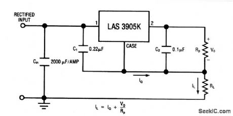
This circuit uses the LAS3905 series voltage regulator (Fig. 7-50) as a fixed-current regulator. Characteristics are shown in Fig. 7-50B, 7-50C, and 7-50D. (View)
View full Circuit Diagram | Comments | Reading(515)
Flash_memory_yorogramming_module_120_mA
Published:2009/7/23 23:53:00 Author:Jessie
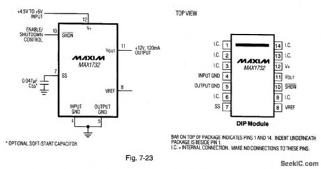
Figure 7-23 shows a MAX1732 connected as a flash-memory programming module. This function is similar to that performed by the circuit of Fig. 7-16, but with only one extemal capadtor required. Quiescent current is 1.7 mA, with 70-μA shutdown current. MAXIM NEW RELEAsES DATA BOOK, 1994, P. 4-15. (View)
View full Circuit Diagram | Comments | Reading(636)
8_A_positive_adjustable_voltage_regulator
Published:2009/7/23 23:53:00 Author:Jessie
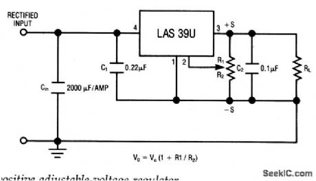
The LAS39U is a four-terminal adjustable-regulator IC with an output range from +4 to + 16 V, providing remote sensing from a single pot.Characteristics are shown in Fig. 7-50B, 7-50C, and 7-50D. (View)
View full Circuit Diagram | Comments | Reading(677)
Basic_F_V_converter
Published:2009/7/23 23:53:00 Author:Jessie
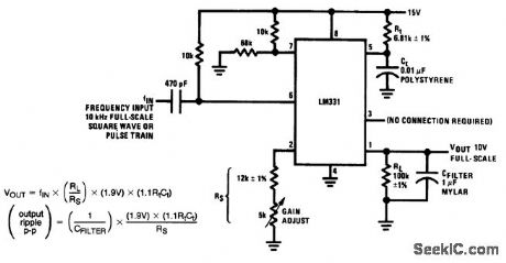
Fig. 12-19 This circuit produces a 10-V output for a 10-kHz full-scale input (square-waves or pulses). Linearity is about 0.06% at full scale. As is the case with most F/V converters, there is a tradeoff between ripple versus response time. With CFILTER at 1μF, as shown, the output ripple is about 13 mVp-p, with a slow 0.6-s settling time. If CFILTER is decreased, the response time is quicker, but ripple increases by the same factor. An increase in CFILTER produces the opposite results. To trim, set the 5-kΩ gain adjust for 10 V out with a 10-kHz input. National Semiconductor, Linear Applications Handbook 1991 p 1253. (View)
View full Circuit Diagram | Comments | Reading(585)
3_A_positive_fixed_current_regulator
Published:2009/7/23 23:24:00 Author:Jessie
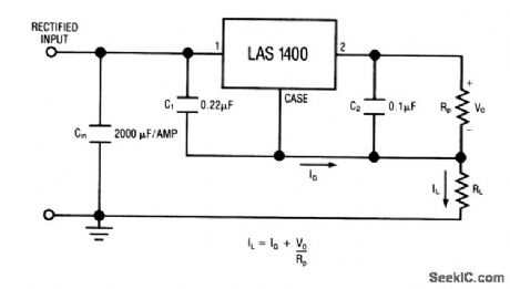
This circuit uses the LAS1400 series voltage regulator (Fig. 7-28A) as a fixed-current regulator. Characteristics are shown in Fig. 7-28B, 7-28C, and 7-28D. (View)
View full Circuit Diagram | Comments | Reading(504)
Quartz_stabilized_V_F_converter_external_clock
Published:2009/7/23 23:23:00 Author:Jessie
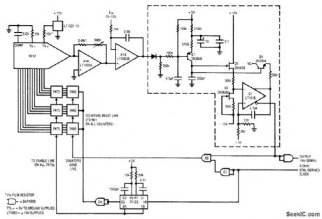
Fig. 12-6 This circuit requires an external4-kHz clock, but it provides very high linearity (typically 0.025%, limited by the 6012 DAC). Range is 1 Hz to 30 MHz, with a typical full-scale drift of 50 ppm/℃, and a zero-point error of about 0.3μV/℃. The circuit is trimmed at the 30-MHz end with the 5000-0 feedback resistor of A1A. Linear Technology linear Applications Handbook, 1990 p AN13-11. (View)
View full Circuit Diagram | Comments | Reading(596)
| Pages:139/291 At 20121122123124125126127128129130131132133134135136137138139140Under 20 |
Circuit Categories
power supply circuit
Amplifier Circuit
Basic Circuit
LED and Light Circuit
Sensor Circuit
Signal Processing
Electrical Equipment Circuit
Control Circuit
Remote Control Circuit
A/D-D/A Converter Circuit
Audio Circuit
Measuring and Test Circuit
Communication Circuit
Computer-Related Circuit
555 Circuit
Automotive Circuit
Repairing Circuit