PCK12429, PCK12429A, PCK12429AA Selling Leads, Datasheet
MFG:PHI Package Cooled:PLCC/28 D/C:02+03

PCK12429, PCK12429A, PCK12429AA Datasheet download

Part Number: PCK12429
MFG: PHI
Package Cooled: PLCC/28
D/C: 02+03


MFG:PHI Package Cooled:PLCC/28 D/C:02+03

PCK12429, PCK12429A, PCK12429AA Datasheet download

MFG: PHI
Package Cooled: PLCC/28
D/C: 02+03
Want to post a buying lead? If you are not a member yet, please select the specific/related part number first and then fill the quantity and your contact details in the "Request for Quotation Form" on the left, and then click "Send RFQ".Your buying lead can then be posted, and the reliable suppliers will quote via our online message system or other channels soon.
TOP
PDF/DataSheet Download
Datasheet: PCK12429
File Size: 132003 KB
Manufacturer: PHILIPS [Philips Semiconductors]
Download : Click here to Download
PDF/DataSheet Download
Datasheet: PCK12429A
File Size: 132003 KB
Manufacturer: PHILIPS [Philips Semiconductors]
Download : Click here to Download
PDF/DataSheet Download
Datasheet: PCK111
File Size: 67168 KB
Manufacturer: PHILIPS [Philips Semiconductors]
Download : Click here to Download
The internal oscillator uses the external quartz crystal as the basis f its frequency reference. The output of the reference oscillator isdivided by 16 before being sent to the phase detector.
The VCO output is scaled by a divider that is configured by eitherthe serial or parallel interfaces. The output of this loop divider is alsoapplied to the phase detector.
The phase detector and loop filter attempt to force the VCO outputfrequency to be M times the reference frequency by adjusting theVCO control voltage. Note that for some values of M (either too highor too low) the PLL will not achieve loop lock.
The output of the VCO is also passed through an output dividerbefore being sent to the PECL output driver. This output divider (Ndivider) is configured through either the serial or the parallelinterfaces, and can provide one of four division ratios (1, 2, 4, or 8).This divider extends performance of the part while providing a 50%duty cycle.
The output driver is driven differentially from the output divider, andis capable of driving a pair of transmission lines terminated in 50 Wto VCC2.0. The positive reference for the output driver and theinternal logic is separated from the power supply for thephase-locked loop to minimize noise induced jitter.
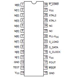
The configuration logic has two sections: serial and parallel. Theparallel interface uses the values at the M[8:0] and N[1:0] inputs toconfigure the internal counters. Normally, on system reset, theP_LOAD input is held LOW until sometime after power becomesvalid. On the LOW-to-HIGH transition of P_LOAD, the parallel inputsare captured. The parallel interface has priority over the serialinterface. Internal pullup resistors are provided on the M[8:0] andN[1:0] inputs to reduce component count in the application of thechip.
The serial interface centers on a fourteen bit shift register. The shiftregister shifts once per rising edge of the S_CLOCK input. Theserial input S_DATA must meet setup and hold timing as specified inthe AC Characteristics section of this document. The configurationlatches will capture the value of the shift register on theHIGH-to-LOW edge of the S_LOAD input. See the programmingsection for more information.
The TEST output reflects various internal node values, and iscontrolled by the T[2:0] bits in the serial data stream. See theprogramming section for more information.

