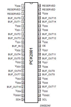
Features: • HIGH speed, LOW noise non-inverting 118 buffer• Typically used to support four SDRAM DIMMs• Multiple VDD, VSS pins for noise reduction• 3.3V operation• Separate 3-State pin for testing• ESD protection exceeds 2000V per Standard 801.2• Optimized...
PCK2001: Features: • HIGH speed, LOW noise non-inverting 118 buffer• Typically used to support four SDRAM DIMMs• Multiple VDD, VSS pins for noise reduction• 3.3V operation• Sepa...
SeekIC Buyer Protection PLUS - newly updated for 2013!
268 Transactions
All payment methods are secure and covered by SeekIC Buyer Protection PLUS.
SYMBOL |
PARAMETER |
CONDITION |
LIMITS
|
UNIT | |
MIN |
MAX |
||||
VDD |
DC 3.3 V supply voltage |
0.5 |
+4.6 |
V | |
IIK |
DC input diode current |
VI < 0 |
- |
50 |
mA |
VI |
DC input voltage |
Note 2 |
0.5 |
5.5 |
V |
IOK |
DC output diode current |
VO > VDD or VO < 0 |
- |
±50 |
mA |
VO |
DC output voltage |
Note 2 |
0.5 |
VCC + 0.5 |
V |
IO |
DC output source or sink current |
VO . 0 to VDD |
- |
±50 |
mA |
Tstg |
Storage temperature range |
65 |
+150 |
°C | |
Ptot |
Power dissipation per package plastic medium-shrink SO (SSOP) |
For temperature range: 0 to +70 °C above +55 °C derate linearly with 11.3 mW/K |
- |
850 |
mW |
NOTES:
1. Stresses beyond those listed may cause permanent damage to the device. These are stress ratings only and functional operation of the device at these or any other conditions beyond those indicated under "recommended operating conditions" is not implied. Exposure to absolute-maximum-rated conditions for extended periods may affect device reliability.
2. The input and output voltage ratings may be exceeded if the input and output current ratings are observed.
The PCK2001 is a 118 fanout buffer used for 133/100 MHz CPU, 66/33 MHz PCI, 14.318 MHz REF, or 133/100/66 MHz SDRAM clock distribution. 18 outputs are typically used to support up to 4 SDRAM DIMMS commonly found in desktop, workstation or server applications.
All clock outputs of PCK2001 meet Intel's drive, rise/fall time, accuracy, and skew requirements. An I2C interface is included to allow each output to be enabled/disabled individually. An output disabled via the I2C interface will be held in the LOW state. In addition, there is an OE input which 3-States all outputs.