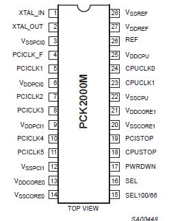
Features: • Reduced pincount version of PCK2000 for mobile applications• Mixed 2.5V and 3.3V operation• Two CPU clocks at 2.5V• Six synchronous PCI clocks at 3.3V, one freerunning• One 3.3V reference clock @ 14.318 MHz• Reference 14.31818 MHz Xtal oscillator inp...
PCK2000M: Features: • Reduced pincount version of PCK2000 for mobile applications• Mixed 2.5V and 3.3V operation• Two CPU clocks at 2.5V• Six synchronous PCI clocks at 3.3V, one freeru...
SeekIC Buyer Protection PLUS - newly updated for 2013!
268 Transactions
All payment methods are secure and covered by SeekIC Buyer Protection PLUS.
SYMBOL |
PARAMETER |
CONDITION |
LIMITS
|
UNIT
| |
MIN |
MAX | ||||
VDD3 |
DC 3.3 V core supply voltage |
0.5 |
+4.6 |
V | |
VDDQ3 |
DC 3.3 V I/O supply voltage |
0.5 |
+4.6 |
V | |
VDDQ2 |
DC 2.5 V I/O supply voltage |
0.5 |
+3.6 |
V | |
IIK |
DC input diode current |
VI < 0 |
-50 |
mA | |
VI |
DC input voltage |
Note 2 |
0.5 |
+5.5 |
V |
IOK |
DC output diode current |
VO > VCC or VO < 0 |
±50 |
mA | |
VO |
DC output voltage |
Note 2 |
-0.5 |
VCC + 0.5 |
V |
IO |
DC output source or sink current |
VO >= 0 to VCC |
- |
±50 |
mA |
TSTG |
Storage temperature range |
65 |
+150 |
°C | |
Ptot |
Power dissipation per package plastic medium-shrink SO (SSOP) |
For temperature range: 0 to +70°Cabove +55°C derate linearly with 11.3mW/K |
- |
850 |
mW |
NOTES:
1. Stresses beyond those listed may cause permanent damage to the device. These are stress ratings only and functional operation of the device at these or any other conditions beyond those indicated under "recommended operating conditions" is not implied. Exposure to absolute-maximum-rated conditions for extended periods may affect device reliability.
2. The input and output voltage ratings may be exceeded if the input and output current ratings are observed.
The PCK2000M is a clock synthesizer/driver chip for a Pentium Pro r other similar processors, typically used in mobile applications.
The PCK2000M has two CPU clock outputs at 2.5V. There are six CI clock outputs running at 33 MHz. One of the PCI clock outputs s freerunning. The 3.3V reference clock outputs at 14.318 MHz. ll clock outputs meet Intel's drive strength, rise/fall time, jitter, ccuracy, and skew requirements.
The part possesses dedicated powerdown, CPUSTOP, and CISTOP input pins for power management control. These inputs of PCK2000M re synchronized onchip and ensure glitchfree output transitions. hen the CPUSTOP input of PCK2000M is asserted, the CPU clock outputs are riven LOW. When the PCISTOP inputs is asserted, the PCI clock utputs are driven LOW.
Finally, when the PWRDWN input pin is asserted, the internal eference oscillator and PLLs are shut down, and all outputs are riven LOW, except the free running PCICLK_F clock output. he PCK2000M is available in a 28pin SSOP package.