
Circuit Diagram
Index 466
555 Voltage monitor circuit
Published:2011/8/4 21:56:00 Author:Ecco | Keyword: 555 , Voltage , monitor
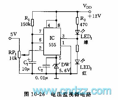
As shown in figure 10-26, the monitoring circuit is an one-shot trigger circuit which is composed of 555 and R1, C1, RP1, DW. Icon monitoring voltage is +5 V, when the input voltage of pin 2 of 555is normal, pin 3 of 555 is in low level, LED1 (green) is lit; if the input voltage is below the seting threshold level, 555 sets, pin 3 is in high level, LED1 is off, LED2 (red) is lit. If the monitor voltageis lower than normal value for a long time, 555 monostable circuit can be continuously re-trigger, that means it will start again after trigger temporary steady state td = 1.1R1C1. Temporary stabilization time of the icon parameter is about 1.7 seconds.
(View)
View full Circuit Diagram | Comments | Reading(2787)
555 Low power, high voltage and low current inverter circuit
Published:2011/8/4 21:55:00 Author:Ecco | Keyword: 555, Low power , high voltage , low current, inverter
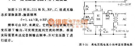
As shown in Figure 9-35, 555 and R1, RP1, C1 form an astable multivibrator, the oscillation frequency f = 1.44 / (R1 +2 R2) C1. The frequency can be adjusted by RP1. Its output is output by the audio step-up transformer T, it may realize the conversion of DC to AC. Selecting the audio output frequency and designing transformer T is according to the actual needs.
(View)
View full Circuit Diagram | Comments | Reading(2389)
The eggs hatching incubator circuit diagram 1
Published:2011/9/18 21:15:00 Author:Ecco | Keyword: Eggs hatching incubator

The eggs hatching incubator circuit is composed of the power supply circuit, temperature detection control circuit and indication circuit, and it is shown in Figure 4-4. Power supply circuit consists of the power switch S, power transformer T, rectifier diodes VDl-VD4 and filter capacitor C. Temperature detection control circuit consists of electric contact thermometer Q, resistor Rl, transistor V, Relay K, diode VD5, thyristors VT1, VT2, and the fan motor M. Indicating circuit consists of resistors R2, R3 and neon lights HLl, HL2. Rl-R3 select the 1/4W metal film resistors. C select the aluminum electrolytic capacitor with voltage in 25V.
(View)
View full Circuit Diagram | Comments | Reading(1903)
USB to parallel, serial circuit diagram(ch341)
Published:2011/9/18 21:34:00 Author:Ecco | Keyword: USB , parallel, serial


View full Circuit Diagram | Comments | Reading(6640)
Hard disk control circuit and the original program
Published:2011/9/18 23:03:00 Author:Ecco | Keyword: Hard disk, control circuit , original program

In the program, all hardware-related parameters is defined at the beginning of the program, when it is transplanted to other types of microcontrollers, the pins defination needs to be simplily changed. When it is used, the corresponding parameters need to be modified according to your hard (there are comments in the program). Firstly, you should connect the circuit (very simple), then the chip is burned into the process. Firstly ,the hard is connected to power, and then you can open any serial debugger to set the baud rate in 57600bps, and then you can run the microcontroller.
(View)
View full Circuit Diagram | Comments | Reading(1508)
DC capacitor tester circuit diagram composed of 555
Published:2011/9/18 22:37:00 Author:Ecco | Keyword: DC , capacitor , tester , 555, 10NF, 100NF, 100PF

DC capacitor tester circuit diagram composed of 555 is shown as the chart. The tester is composed of the pulse generator, one-shot, DC amplifier and meter indication circuit. It can measures the npF ~ 10μF capacitor. The range is divided into 0 ~ 100PF, 0 ~ 1nF, 0 ~ 10nF, 0 ~ 100nF, 0 ~ 1μF, 0 ~ 10μF.
(View)
View full Circuit Diagram | Comments | Reading(5661)
The current loop interface circuit diagram of AD694 being used as D / A converter
Published:2011/9/18 22:35:00 Author:Ecco | Keyword: current loop , interface circuit, D / A converter

The current loop interface circuit diagram of AD694 multi-functional sensor signal conditioner being used as D / A converter.
The current loop interface of AD694 being used as D / A converter (DAC) can achieve the conversion of digitalvalue →voltage signal →current signal . DAC's current loop interface circuit is shown as the chart. AD566A is high-speed 12-bit DAC, its output (DAC OUT) is connected to AD694's UI-end, UI + is grounded. AD694 uses ± 15V dual supplies, and provides reference voltage to the AD566A. Internal resistor network of AD566A will set AD694 with 10V full scale input. C2 is the frequency compensation capacitor. RP is the full scale adjusting potentiometer, it has no need to use a fixed adjustment 50Ω resistor to replace the potentiometer.
(View)
View full Circuit Diagram | Comments | Reading(2697)
The LA4505 IC typical application circuit
Published:2011/9/19 1:32:00 Author:Ecco | Keyword: typical application , IC

The typical application circuit
The typical application circuit of LA4505 IC is shown as the chart, the left and right audio signalsare input from the foot and pin ⑧ of LA4505 and it is amplified and output from ④ feet to drive the speaker power, and the power can reach ten 8W +8W (RL30).
(View)
View full Circuit Diagram | Comments | Reading(4151)
Integrated circuit diagram of TDA9112-I2C bus control row / field scanning
Published:2011/9/19 1:18:00 Author:Ecco | Keyword: bus control, row , field , scanning , integrated circuit


TDA9112 is the bus control row / field scanning integrated circuit produced by Philips, it is widely used in color displays, such as color display of Tsinghua Tongfang. 1. Featuresand functionTDA9112 IC includes I2C bus interface circuit, the line oscillator circuit, field oscillation and the sawtooth wave generating circuit, left and right pincushion correction circuit, the line excitation circuit, PLL circuit, the same frequency signal processing circuit, ABL beam current system circuit, X-ray protection circuit, and other auxiliary functions circuit. 2. Pin functions and dataTDA9112 IC uses 32-pin dual in-line package, the pin functions and the number are shown in Table 1. Table 1 shows TDA9112 integrated circuit pin functions and data.
(View)
View full Circuit Diagram | Comments | Reading(924)
The driver circuit diagram of glow numerating tube
Published:2011/9/19 1:17:00 Author:Ecco | Keyword: glow numerating tube , driver circuit

The glow numerating tube can be driven by a strong electric field, so it needs to be equipped with an electronic switch between decoder and the glow digital tube. The VT1-VT10 shown in the circuit is the switch circuit that composed of transistors. (View)
View full Circuit Diagram | Comments | Reading(1278)
555 Inductive battery charging circuit
Published:2011/9/18 21:15:00 Author:Ecco | Keyword: 555, Inductive , battery, charging circuit
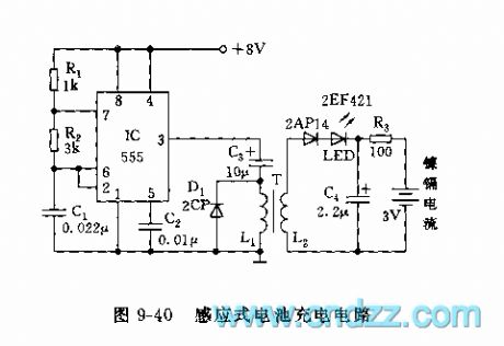
As shown in Figure 9-40, 555 and R1, R2, C1 form an astable multivibrator, f = 1.44/ (R1 +2 R2) C1, the oscillation frequency of the icon parameter is approximately 10kHz. The oscillation square wave is added to the primary L1, secondary L2 of inductively coupled coil, and two nickel-cadmium batteries are mounted in the dielectric plexiglass shell, that is, it uses inductive charging method. The core of coil antenna uses φ10 magnet bar of radio, it uses φ0.13mm and φ0.27mm wires with 200turns on the primary and secondary coils, the middle is cut and connected in the both sides of dielectric plexiglass panels. Battery charging current is up to 10mA, when it is charging, LED is lit.
(View)
View full Circuit Diagram | Comments | Reading(5923)
555 pointer electronic megohmmeter
Published:2011/9/18 21:14:00 Author:Ecco | Keyword: 555 , pointer electronic megohmmeter
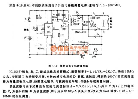
As shown in Figure 8-19, the megohmmeter uses the electronic boost circuit as measuring power, the range is 0.5 ~ 1000MΩ. IC1 and R1, R2, C1 are connected in non-steady-state oscillation mode, and the oscillation frequency f = 1.44 / (R1 +2 R2) C1, it is about 15kHz. Transformer T is the step-up transformer, the secondary induced voltage is rectified by D1, after being filtered, it can get 1000V DC high voltage power supply as measuring voltage, the current limiting resistor R5 and the measured resistor are connected in series and then form measuring loop with header. Dial readings can be calculated by the following formula, the current value of the corresponding label: I = V / (R + R5 + Rg), and V is the voltage on C5, Rg is the internal resistance of meter, R is the dial reading. RP1 header is used for for streaming on the 100μA header, correcting 2mA full-scale, and measuring low resistor with 0.5 ~ 10MΩ.
(View)
View full Circuit Diagram | Comments | Reading(3463)
555 resistance quick measuring circuit
Published:2011/9/18 21:12:00 Author:Ecco | Keyword: 555, resistance quick measuring

As shown in Figure 7-8, measuring circuit uses 555 as the core, and 555,R1, R2, R3, Rx, C1 form an astable multivibrator.
Changing the switch K can change the oscillation frequency. Since R4 ~ R9 resistor (10Ω ~ 1MΩ) is known, Rx is the resistance under test,it caneasily and quickly determine the resistance of Rx by the comparison of the sound with correspondingoscillation frequency of known resistors.
(View)
View full Circuit Diagram | Comments | Reading(1877)
100w VMOS tube inverter power supply circuit
Published:2011/9/18 21:11:00 Author:Ecco | Keyword: 100w , VMOS tube, inverter power supply

As shown in Figure 4-11, the circuit is composed of 555 trigger and step-down rectifier circuit. When the hands touch metal A, the sensor signals make the internal comparator 555 turn and set, K pulls, the contact K1-1 closes; if people touch A again, K releases.
(View)
View full Circuit Diagram | Comments | Reading(1616)
555 AC timing switch controller circuit
Published:2011/9/18 22:13:00 Author:Ecco | Keyword: 555 , AC, timing switch , controller
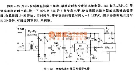
As shown in Figure 4-22, the controller includes the buck rectifier, monostable AC solid relay. And 555 and R1, RP1, C4, etc. form a monostable circuit, clicking the AN, the pin 3 of 555 is in high level, the AC output of AC solid relay turns on, load is connected, timing begins. Regular time is the monostable transient stability time td = 1.1RP1C4, the longest time of icon argument is about 30 minutes, it can be adjusted by RP1.
(View)
View full Circuit Diagram | Comments | Reading(1470)
Generator circuit of 555 square wave and sawtooth wave
Published:2011/9/18 22:06:00 Author:Ecco | Keyword: 555 , square wave , sawtooth wave, generator circuit
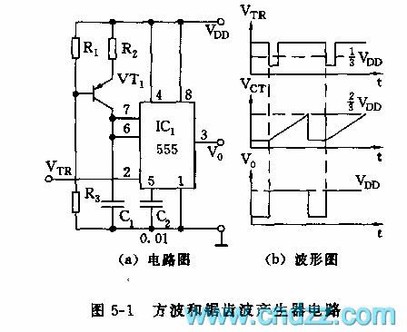
As shown in Figure 5-1, 555 and R2, C1, VT1 form a monostable trigger circuit, and the difference from the general flip-flop is that VT1, R1, R2, R3 form a constant current source, which charges for C1 to make a good voltage linearity, accurate delay. Delay time td = 1.1R2C1. If it requires trigger pulse period T to be greater than td, the output waveform is shown in Figure b.
(View)
View full Circuit Diagram | Comments | Reading(1444)
555 various waveform generator circuit 1
Published:2011/9/18 22:04:00 Author:Ecco | Keyword: 555, various waveform, generator
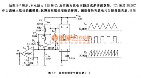
The circuit shown in Figure 5-7 is a multi-vibrator circuit composed of 555 and constant current charging and discharging circuit and C1. IC2 uses 5G28C as a high input impedance follower to play the role of isolation and impedance transformation. Oscillators are constant current charging and discharging, so the sawtooth has a good linearity. RP1, RP2 are used to adjust the charging and discharging time constant and the duty cycle. Icon parameter cycle is 0.2ms ~ 60s. When K1 is closed, it produces sawtooth, of which period is half the triangle wave.
(View)
View full Circuit Diagram | Comments | Reading(2430)
555 Linear voltage / frequency converter circuit 4
Published:2011/9/18 22:03:00 Author:Ecco | Keyword: 555, Linear voltage , frequency , converter

As shown in Figure 5-37, IC1 and R1, C1, D1, etc form integrator, 555 and R2, C2 etc. form monostable trigger. When the input voltage Vi changes in the range of 0 ~ 10V, the 1kHz / V conversion factor of VFC circuit can be transformed into 0 ~ 10kHz frequency. When there being the input signal voltage Vin, IC1 output declines to the trigger level of IC2, 555 sets, VT2 is conducted, D2, D3 are cut off, D1 turns on, VT1 provides constant current andanti-charge for C1. IC1's output voltage rises. At this point, IC2 monostable timing capacitor C2 charges to 2/3 VDD threshold level, the 555 resets, VT2 is off, D2, D3 are conducted, D1 closes, the input voltage is converted to a certain frequency of oscillation again and again.
(View)
View full Circuit Diagram | Comments | Reading(1443)
555 Linear voltage / frequency converter circuit 3
Published:2011/9/18 21:48:00 Author:Ecco | Keyword: 555, Linear voltage , frequency , converter

As shown in Figure 5-36, the linear voltage/frequency converter is a practical voltage/frequency converter. When added to the input voltage, the voltage on C1 increases linearly, when it is reached 2/3 VDD, the 555 flip sets, VT1 is conducted, C1 quickly discharges. Round trip time is also associated with the R5,C3 time constant, that is, when the voltage of C3 decreases to 1/3 VDD, the 555 sets. VT1 is cut off, then it starts the next time. The circuit's return time is about 1μs. When the frequency is over 10KHz, the nonlinear error is about 0.2%.
(View)
View full Circuit Diagram | Comments | Reading(2333)
555 Linear voltage / frequency converter circuit 2
Published:2011/9/18 21:47:00 Author:Ecco | Keyword: 555 , Linear voltage, frequency converter

As shown in Figure 5-35, the converter is composed of in-phase amplifier, integrator and oscillator. It is usedfor voltage and frequency conversion. IC1 operational amplifier is connected as an inverting amplifier, the voltage is dropped to the trigger level of 555, 555 sets. At the same time, VT1 is conducted, integration capacitor discharges rapidly, the integrator voltage V2 charges for C2 through R9, when the voltage of C2 rises up to 2/3 VDD, 555 resets, then it forms shocks. Therefore, the input voltage is changed into shock wave with a certain frequency. When the input signal voltage is in the 0 ~ V, the output frequency is 10HZ ~ 10kHz.
(View)
View full Circuit Diagram | Comments | Reading(2710)
| Pages:466/2234 At 20461462463464465466467468469470471472473474475476477478479480Under 20 |
Circuit Categories
power supply circuit
Amplifier Circuit
Basic Circuit
LED and Light Circuit
Sensor Circuit
Signal Processing
Electrical Equipment Circuit
Control Circuit
Remote Control Circuit
A/D-D/A Converter Circuit
Audio Circuit
Measuring and Test Circuit
Communication Circuit
Computer-Related Circuit
555 Circuit
Automotive Circuit
Repairing Circuit