
Circuit Diagram
Index 479
SAA3010 Typical application circuit
Published:2011/9/13 21:24:00 Author:Ecco | Keyword: Typical application
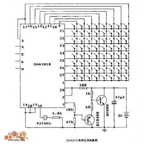
View full Circuit Diagram | Comments | Reading(2107)
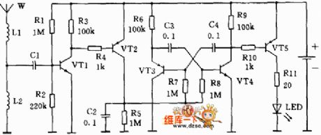
HA1377 dual-channel working typical application circuit
Published:2011/9/14 1:59:00 Author:Ecco | Keyword: dual-channel working , typical application

View full Circuit Diagram | Comments | Reading(572)
900MHz radio frequency indicator analysis circuit diagram
Published:2011/9/13 20:39:00 Author:Ecco | Keyword: 900MHz, radio frequency indicator, analysis
When the phone receives the signal sent by the base station in standby mode, it will send response signal, and cell phone antenna also has a short radio signal. At this point, if there is a tiny sensor next to the phone, it will emit red light, and some sensor will issue music, sound. Anatomy sensor circuit is actually a 900MHz radio frequency indicator. When there is no RF signal near the phone antenna, all will restore quiet. R1's size is relative to the magnification of VT1.
(View)
View full Circuit Diagram | Comments | Reading(1804)
AC contactor power saving noiseless operation circuit
Published:2011/9/14 21:26:00 Author:Christina | Keyword: AC, contactor, power saving, noiseless operation

View full Circuit Diagram | Comments | Reading(1372)
LA7837 Field scanning output IC
Published:2011/9/13 20:18:00 Author:Ecco | Keyword: Field scanning output IC

LA7837 field scanning output IC produced by Japan's Sanyo is widely used in domestic and imported color TV. 1. Features and functions LA7837 IC includes field oscillation and sawtooth generator circuit, field excitation and output circuit. The maximum output current is 1.8 AP-P, and the maximum output power is 8W, then the manifold internal block diagram and typical application circuit are shown in Figure 1. 2. pin functions and data LA7837 IC pin functions and data are listed in Table 1-2.
(View)
View full Circuit Diagram | Comments | Reading(5797)
Regulator power supply circuit with adjutable power which is formed by L431
Published:2011/9/15 20:02:00 Author:leo | Keyword: Regulator, power supply, adjutable power

As the picture 1 shows, this is regulator power supply circuit with adjustable power. Its output voltage can reach 36 V and the current can reach 0.1 mA. Its dynamic resistance is 0.22ohm. The picture 2 shows the classic applying of the TL431. The voltages of pin 2 and pin 2 V are the value getting from the format :2.5x(R2十R3)V/R3.If the value of R2 is changed, the output base voltage will also be changed. And the picture 3 shows the classic application of the adjusting tune formed by the base voltage and driving MOFET k790, which can output about 6 A current. This circuit is a simple and safe regulator power supply one. (View)
View full Circuit Diagram | Comments | Reading(1327)
Typical application circuit diagram of BTL connection
Published:2011/9/13 20:43:00 Author:Ecco | Keyword: Typical application, BTL connection

View full Circuit Diagram | Comments | Reading(959)
MAX262 Programmable filter circuit
Published:2011/9/13 21:15:00 Author:Ecco | Keyword: Programmable filter
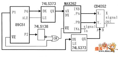
Programmable filter is mainly achieved by the MAX262. MAX262 achieves programmable filter from filter parameters programmed by the SPI bus, and the center frequency and quality factor are 64, 128-level programming adjustable, the circuit is shown as the chart.
(View)
View full Circuit Diagram | Comments | Reading(855)
High-fidelity audio power amplifier LM1875 circuit diagram
Published:2011/9/13 21:16:00 Author:Ecco | Keyword: High-fidelity , audio power amplifier


View full Circuit Diagram | Comments | Reading(3817)
The full-wave rectifier circuit of high-frequency response using balanced output transformer
Published:2011/9/15 0:02:00 Author:Sophia | Keyword: The full-wave rectifier circuit, high-frequency response, balanced output transformer

When measuring AC signal levels, the AC circuit is converted into DC, which is called rectifier circuit. But in the rectifier circuit with the diode, the diode forward voltage is very annoying, so a variety of the rectifier circuits appear with the purpuse to remove the effects of the diode forward voltage.
Low-frequency full-wave rectifier circuit is mentioned above, which can be easily achieved through a combination of OP amplifiers and diode, but because the OP amplifier band is very low, we can not achieve the precision rectifier. (View)
View full Circuit Diagram | Comments | Reading(2537)
Low frequency compensation circuit of current transformer
Published:2011/9/15 0:02:00 Author:Sophia | Keyword: Low frequency compensation, current transformer

Figure 1 shows the circuit, when the OP amplifier A as the current is inputed into amplifier and visible load resistance R of CT is 0. This circuit can significantly improve the low frequency characteristics. When the gain of low-frequency domain needs to be compensated, the feedback capacitor CF can be inserted into . In this circuit, to prevent the OP amplifier A becoming into open-loop in the DC area and composing of the DC open-loop (fc ≈ 1.6Hz) in the non-inverting integrator A2 (commonly known as the DC servo circuit), this circuit's output voltage v is:
If RF = 50kΩ, then i = 10mA, which can be transformed as 1V.
The value of this capacitor CF is decided by the CF characteristics of short-circuit, so it can be obtained by the experiment. The 47pF capacitor parallelling with FR is to suppress high-frequency characteristics, no special basis. (View)
View full Circuit Diagram | Comments | Reading(5163)
Feedback resistance circuit diagram of current feedback operational amplifier
Published:2011/9/15 0:01:00 Author:Sophia | Keyword: Feedback resistance, current feedback, operational amplifier

About the current feedback operational amplifier, even if the open-loop gain was changed, the bandwidth also will not be changed. It is often used in video signal amplificaion and the drive circuit of video cable. The diagram is a vedio inphase amplification circuit.
If the broadband high-speed voltage feedback op amp AD844 is adopted, it need to have a phase compensation with the feedback resistor RF and shunt capacitor C. Capacitor C is used to limit the bandwidth, but also have a strong capacity on the capacitive load.
If the current feedback op amp AD844 is adopted and is in parallel with the capacitance C with resistor RF. the circuit will not be stable.
(View)
View full Circuit Diagram | Comments | Reading(1696)
Switch off isolation circuit diagram
Published:2011/9/14 23:48:00 Author:Sophia | Keyword: Switch off, Isolation

Conversion signal switches include mechanical switches, relays, analog switches. The frequency of the signal must be paid attention to when choosing these switches, not only the signal frequency through the switch need to be paid attention to when the switch is turned on, but also the signal via the switch leakage frequency need to be paid attention to when the switch is off, that is the isolation when switch is off. Figure is a the measurement circuit of the isolation when variety of small-signal switches are off. When frequency is 1MHZ, for mechanical switches and analog switches, the isolation is about 30dB, for the relay, it is about 25dB. Due to the impact of the switch construction and distributed capacitance within the switch, the isolation will become low. Therefore, the circuit construction can be considered to improved. high-frequency signal dedicated switch with enough isolation can be adopted. (View)
View full Circuit Diagram | Comments | Reading(1040)
MAX157/MAX1577Z charger-pump drive white light LED
Published:2011/9/14 21:07:00 Author:leo | Keyword: charger-pump, white light LED
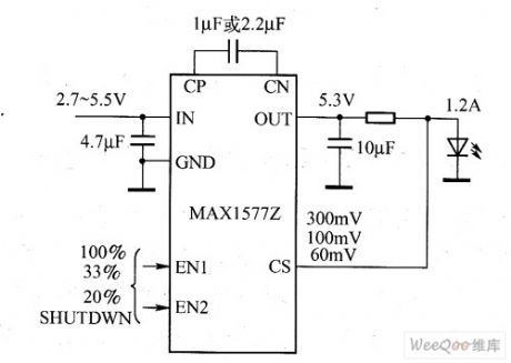
MAX157/MAX1577Z charger-pump is used to drive high power white light LED, for example, camera flash. Its maximum current is 1.2A and minimum current is 800 mA. Even if its input voltage and current are super low, its low resistance will allow it has a high brightness of flash. It adopts outer resistance set system to control the current. Max1577Z has a fixed output voltage of 5.1 V and MAX1577Y can output voltage of 3.4 V, 4.6 V or 5.1 V. (View)
View full Circuit Diagram | Comments | Reading(947)
Circuit of Direct Current Motor Driven by SA60
Published:2011/9/15 0:11:00 Author:Zoey | Keyword: Direct Current, Motor, Carrier frequency
The following picture shows the typical connection circuit of direct current motor driven by SA60. Therein, the chip has been connected to an annalog input circuit. A capacitor is connected between numerical input terminal(pin 2) and analog site. By changingthe capacity, frequency of PWM load can be adjusted, making it range between 22 to 250 kHZ. (View)
View full Circuit Diagram | Comments | Reading(540)
power amplifier(STK6153,STK3048) circuit of thick film integrated package
Published:2011/9/15 1:42:00 Author:chopper | Keyword: power amplifier, thick film, integrated package

The picture is a power amplifition circuit of thick film integrated package.Picture (a) shows that input signal is loaded to in-phase end of STK3048 through resistace-capacity coupling circuit(resistance is 33kΩ,capacitance is 4.7μF) and it is added to the base of power tube Q1,Q2 by its output end after it is amplified by thick film power amplifier STK3048.The power amplifier adopts dynatron 2N3055 and MJ2955.R1,R2(0.25Ω) are protective resistors of common emitter. Adjusting potentiometer RP can make power tube in the stage of classA,B,and at this time,the voltage drop of R1,R2 is about 10~13mV,the quiescent current of corresponding Q1 and Q2 is 40~50mA. (View)
View full Circuit Diagram | Comments | Reading(1262)
simple VSP3010 equivalent input circuit
Published:2011/9/15 1:43:00 Author:chopper | Keyword: simple, equivalent input

VSP3010 is one of appropriative integrated chips thatare produced by company Burr-Brown and it is used to process CCD signals.It can process signals from channel 1 or channel 3.Each channel has the capability of signal sampling,black level adjustment and programmable gain amplification and then enter 12-bit A/ D whose sampling rate is 12 MHz through multiple selector.Its single-channel signal processing circuit is as following picture. (View)
View full Circuit Diagram | Comments | Reading(592)
Audi Cruise Control circuit
Published:2011/9/14 21:02:00 Author:John | Keyword: Cruise Control

View full Circuit Diagram | Comments | Reading(1322)
HST Hall sensor common application interface circuit
Published:2011/9/14 21:02:00 Author:John | Keyword: sensor, application interface

View full Circuit Diagram | Comments | Reading(1595)
Integrated circuit inside circuit box circuit
Published:2011/9/14 21:01:00 Author:John | Keyword: Integrated circuit, inside circuit

Features
LM331 integrated circuit is a precision frequency - voltage (also voltage - frequency) converting circuit. It includes power switch circuit, precision current source, reference power, timing comparator, RS flip-flop, input comparator, protection circuit and some other auxiliary circuit. The inside circuit box circuit is just as shown.
(View)
View full Circuit Diagram | Comments | Reading(1544)
| Pages:479/2234 At 20461462463464465466467468469470471472473474475476477478479480Under 20 |
Circuit Categories
power supply circuit
Amplifier Circuit
Basic Circuit
LED and Light Circuit
Sensor Circuit
Signal Processing
Electrical Equipment Circuit
Control Circuit
Remote Control Circuit
A/D-D/A Converter Circuit
Audio Circuit
Measuring and Test Circuit
Communication Circuit
Computer-Related Circuit
555 Circuit
Automotive Circuit
Repairing Circuit