
Circuit Diagram
Index 467
555 Dual astable multivibrator circuit
Published:2011/9/18 21:46:00 Author:Ecco | Keyword: 555, Dual , astable , multivibrator
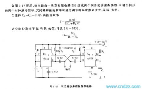
As shown in Figure 3-17, the circuit has two synchronized multivibrators whichare composed of 556 dual time-base circuit, andit can output two clock pulse signals simultaneously, the spacing and oscillation frequency can be changed by adjusting the time constant. When you select C1 = C2 = C, f = 0.91 / (R1 + R2) C, duty cycle depends on the value of R1 and R2 and it can be up to 5% to 95%.
(View)
View full Circuit Diagram | Comments | Reading(2271)
Power factor compensation schematic circuit diagram
Published:2011/9/14 21:11:00 Author:Rebekka | Keyword: Power factor compensation
The controller is divided into measurement part, Enlarged part of the DC, executing part and power supply part by dotted line. The operation is as follows: Converting the phase displacement between AC voltage and current into DC voltage signal. Then making DC driver signal amplification work in sections, theninput or remove to compensation capacitor.
(View)
View full Circuit Diagram | Comments | Reading(1159)
Amblyopia dual digital display therapeutic apparatus circuit diagram
Published:2011/9/14 21:10:00 Author:Rebekka | Keyword: Amblyopia , dual digital display, therapeutic apparatus
View full Circuit Diagram | Comments | Reading(1483)
FM modulation circuit diagram using ceramic resonator
Published:2011/9/14 21:38:00 Author:Rebekka | Keyword: ceramic resonator, FM modulation

On frequency stability, the quartz crystal oscillator circuit is very advantageous, even the the VCXO circuit with large amount of frequency changing only changes about 1%, and the linear range of control voltage to frequency variation is not wide. Although the ceramic resonator Q value is lower than the quartz crystal oscillator, the inductive range is relatively broad, so it can get a wider frequency range, and the characteristics in the frequency stability is also better than the LC oscillator, so it is suitable for wideband FM modulator. (View)
View full Circuit Diagram | Comments | Reading(2947)
Music controlling circuit diagram
Published:2011/8/31 2:46:00 Author:Rebekka | Keyword: Music controlling circuit

The circuit can drive 10 pieces of 40W fluorescent lamps. When K2 is closed, the brightness of the light will change the audio signal amplitude.Because fluorescent lamp has not the time delay effect like incandescent lamp, the music can control the light of dance hall accurately and timely. (View)
View full Circuit Diagram | Comments | Reading(595)
Earthquake sound and light alarm circuit
Published:2011/9/14 21:06:00 Author:Rebekka | Keyword: Earthquake , sound and light , alarm

The circuit is composed of two integrated circuit chips as the core, and it has few external components, but experiments show the favorable results. It's the circuit is shown as the chart. 555 and R2, C1 form a monostable trigger, usually due to the small copper hammer is floating isolated, the pin 2 of 555 is connected to high potential Vnn by R1, thus making 555 be in a reset state, that is, pin 3 outputs low, then the backward stage does not work without electricity. HFC5212 is the high level trigger, and the quiescent current is very small, the working output current I0 is about 1mA, which can directly drive medium, low power tube.
(View)
View full Circuit Diagram | Comments | Reading(611)
btl circuit theory and circuit diagram
Published:2011/9/12 22:21:00 Author:Rebekka | Keyword: btl circuit theory

The working theory circuit diagram is shown as above. There is no direct current in load RL. In the positive half cycle of the ui, the top is positiveand down is negative, V1 and V4 areturned on, V2 and V3 stop, the current passing load RL is shown as the real line in the figure; In the negative halfcycle of the ui, negative is on the top and down is the positive, V1 and V4 stop, V2 and V3 turn on, the current passing load RL is shown as the dotted line in the figure. Ignore saturation voltage, two halfs cycles will be compounded. It can get output signal voltagewith width in UCC from load. (View)
View full Circuit Diagram | Comments | Reading(693)
High power led drive reduction voltage regulator circuit diagram
Published:2011/8/22 22:31:00 Author:Rebekka | Keyword: High power , led driver , reduction voltage regulator

The input voltage in the whole series or series-parallel LED system is higher than the the maximum forward voltage, the best option is the standard power buck regulator topology. Because it has the output sensor, andit is ideal for constant current drive.
In the three standard DC-DC converters(buck, boost and buck - boost), only the buck converter LED driver average load current or IF is equal average inductor current. No matter which controlling method you use, in fact, the output current will not have transient change in any part of the switching loop. This makes it easier to convert the constant voltage source to constant current source. To be more specific, many step-down converters based on constant current circuit can run without output capacitor.
(View)
View full Circuit Diagram | Comments | Reading(1598)
5V fixed voltage power supply circuit diagram with doubler rectifier
Published:2011/8/22 22:31:00 Author:Rebekka | Keyword: doubler rectifier , 5V , fixed voltage , power supply

View full Circuit Diagram | Comments | Reading(1203)
Dual op amp basic subtraction circuit composed of ICL7622
Published:2011/8/22 22:32:00 Author:Rebekka | Keyword: Dual op amp, basic subtraction

Dual op amp basic subtraction circuit composed of ICL7622 is shown as above.
The device used in the circuit is ICL7622 (or CF7622) which is a monolithic CMOS dual op amp dual low-power, and its working power voltage is ± 0.5 ~ ± 8V. The input current is very small. The device also has the features of internal compensation for zero offset, offset fixed and so on. The main typical parameters of ICL7622are shown as above. (View)
View full Circuit Diagram | Comments | Reading(624)
Integrated counter timer timing circuit composed of XR2240
Published:2011/8/22 22:33:00 Author:Rebekka | Keyword: Integrated counter timer, timing circuit

XR2240 is an integrated counter timer. It is an improved device based on 555. It includes an oscillator composed of 555, eight divider and control logic circuit. The XR2240 block diagram and timing diagram is shown as above.
(View)
View full Circuit Diagram | Comments | Reading(1876)
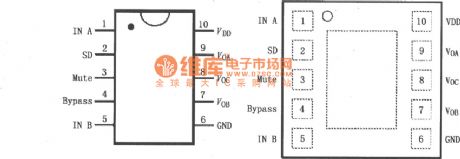
The typical circuit diagram of LM4916 for binaural amplifier
Published:2011/8/22 22:18:00 Author:Rebekka | Keyword: Two-channel amplifier

Pin 1 and 5 of LM4916 are inputed seperately by left and right channel audio signals and outputed respectively by pin 9, 7 after being amplified by the internal amplifier. Through Coupling capacitor Co adding to since channel speaker. The pin 2 of LM4916 connects shutdown control. It is allowed to work when pin 2 connects with VDD; It is not allowed to when it connetcs to a low level or it will decrease chip power consumption. The pin3 of LM4916 is squelch control. It is squelch mode when pin 3 connects to a low level. In order to eliminate the Cameroon - flapping sound that caused by switching transitions. It is allowed to work when it connects to a high level. (View)
View full Circuit Diagram | Comments | Reading(1010)
LM4911 typical application circuit diagram for dual-channel amplifier
Published:2011/8/22 22:16:00 Author:Rebekka | Keyword: MSOP, dual-channel amplifier

Left and right channel audio signals areinputto 1,5 feet of LM4911 (MSOP packaging)respectively. They are output by 9, 7, 8 feet after being amplified by the internal amplifier. They will be added to the respective channel speaker through coupling capacitor. Maximum power of the amplifier is PDMAX = VDD2/2π2RL (output capacitive coupling mode). LM4911's 2 feetis connected shutdown Control outside. It is allowed to work when 2 feet connected VDD (high level). It is not allowed to work when then low (ground) because it will reduce chip power consumption. (View)
View full Circuit Diagram | Comments | Reading(755)
LM4911 OCL output earphone amplifier circuit diagram
Published:2011/8/22 22:16:00 Author:Rebekka | Keyword: OCL output , earphone amplifier
LM4911 is a stereo headphone amplifier with 3.3V power supply. Every channel outputs 40mW that continuous average power drives 16Ω load, or every channel outputs 25mWand continuous average power drives 32Ω load. LM4911 can use single-ended capacitive coupling output or OCL output structure. It has a low-power shutdown mode and power squelch mode. When the release changes in the output voltage is less than 1mV, the breakover turns fast. LM4911 also contains an internal thermal shutdown protection agency, the pin arrangement is shown as the chart.
(View)
View full Circuit Diagram | Comments | Reading(1168)
LM4910 stereo headphone amplifier circuit diagram
Published:2011/8/31 2:32:00 Author:Rebekka | Keyword: stereo headphone amplifier

LM4910 is an audio power amplifier. It is primarily designed for portable devices, and it uses 3.3V power supply. It can output 35mW continuous average power todriver 32Ω load. LM4910 uses new topology circuit to cancle headphone amplifier output coupling capacitor and half-supply bypass capacitor, and it includes an advanced click - flutter noise elimination circuit. This noise generates instantly when you switch it off. LM4910 pinout is shown as the chart.
(View)
View full Circuit Diagram | Comments | Reading(804)
LM4809, LM4810 typical circuit diagram for two-channel headphone amplifier
Published:2011/8/31 2:34:00 Author:Rebekka | Keyword: two-channel headphone amplifier, typical circuit

Left and right channel audio signals are input M4809/4810(SOP/MSOP packaging) 2, 6 feet respectively. They are output by 1, 7 feet after being amplified by the internal amplifier. They will be added to the respective channel speaker through coupling capacitor. Amplifier gain Av = Rf / Ri. LM4809's pin 5 is connected externalshutdown control. when pin 5 is connected to VDD(high level), it is allowed to work; when pin 5 is grounded(low level), it can not work.
(View)
View full Circuit Diagram | Comments | Reading(1604)
LM4809, LM4810 Dual-channel headphone amplifier circuit diagram
Published:2011/8/31 2:35:00 Author:Rebekka | Keyword: Dual-channel , headphone amplifier

LM4809/4810 is dual channel headphone amplifier with 5V power supply. Each channel can output 105mW continuous average power to drive 16Ω load. Total harmonic distortion plus noise (THD + N) is only 0.1%. LM4809/4810 isthe minimum number of external components, which canprovide high-quality output power. LM4809/4810 does not require bootstrap capacitor and buffer. It is qualified to low-power portable systems. LM4809/4810 has an external control terminal to produce effectivelow level shutdown mode to work in the micro-power. There is an internal thermal shutdown protection agency. The pinout is shown as the chart.
(View)
View full Circuit Diagram | Comments | Reading(1023)
TDA2002, TDA2003 8W Audio power amplifier circuit diagram
Published:2011/8/31 2:35:00 Author:Rebekka | Keyword: 8W , Audio power amplifier

View full Circuit Diagram | Comments | Reading(3662)
TDA1512, TDA1512Q 20WHi-Fi audio power amplifier circuit diagram
Published:2011/8/31 2:36:00 Author:Rebekka | Keyword: 20WHi-Fi , audio power amplifier

View full Circuit Diagram | Comments | Reading(2109)
Gain programmable low noise differential amplifier circuit composed of OPA37
Published:2011/8/31 2:38:00 Author:Rebekka | Keyword: Gain programmable low noise, differential amplifier


Total gain Av and A0, A1 corresponding relation:
The main parameters of the OPA27 integrated chips (typical values):
The figure shows the gain programmable low noise differential amplifier circuit. The circuit is composed of two parts: The first level differential input consists of the two pieces of OPA27 high precision low noise op-amps , the second level is composed of the numerical control gain programming instrument amplifier PGA203.
(View)
View full Circuit Diagram | Comments | Reading(673)
| Pages:467/2234 At 20461462463464465466467468469470471472473474475476477478479480Under 20 |
Circuit Categories
power supply circuit
Amplifier Circuit
Basic Circuit
LED and Light Circuit
Sensor Circuit
Signal Processing
Electrical Equipment Circuit
Control Circuit
Remote Control Circuit
A/D-D/A Converter Circuit
Audio Circuit
Measuring and Test Circuit
Communication Circuit
Computer-Related Circuit
555 Circuit
Automotive Circuit
Repairing Circuit