
Circuit Diagram
Index 1539
TDA8946J pin functions and power amplification circuit diagram
Published:2011/6/27 2:17:00 Author:Ecco | Keyword: pin functions , power amplification
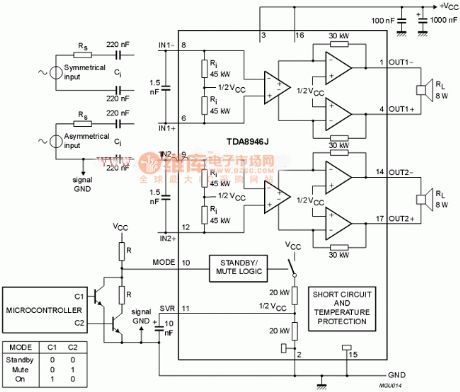
TDA8946J is a dual audio power amplifier, which contains two BTL amplifier circuits. When the power supply voltage is 18V, the load is 8 ohms, it can output 2 X 15W effective power. TDA8946J is packaged with ZIP dual in-line with the power supply range in 6 ~ 25V. THD total harmonic distortion is 0.03 0.1. 1. negative output terminal; 2. ground; 3. supply voltage VCC1; 4. output terminal; 5. empty; 6. the input signal; 7. empty; 8. input 1 is negative; 9. signal input 2 is negative; 10 . squelch control (alternate); 11. ripple rejection (external connected 10nF capacitor to ground); 12. signal input 2 is positive ; 13. empty; 14. output terminal 2 is negative; 15. ground; 16. power supply voltage VCC2; 17. output Terminal 2 is positive.
(View)
View full Circuit Diagram | Comments | Reading(5379)
Class A discrete component amplifier circuit diagram
Published:2011/6/26 21:58:00 Author:Ecco | Keyword: Class A , discrete component , amplifier
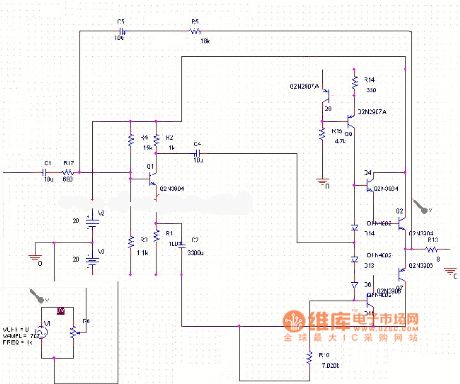
This amplifier circuit uses the dual 20V power supply voltage to provide 15W power without distortion at the 8 ohm load. Q1 operates in the common emitter, and the input signal can provide constant current bias through the bias tube, which is including Q8, Q9, D6, D13 and D14. Q8 and Q9, and the product phase is minimized by the separation darlington tubes (Q2, q4) and (Q7, q11). The two transistors uses Transitors, specifically the types of 2N3055 and MJ2955. R16 uses the series of 4.7K, 680 Ohms and 820 ohm resistors.
(View)
View full Circuit Diagram | Comments | Reading(931)
Multi-function digital multimeter TC821 integrated circuit diagram
Published:2011/6/27 1:23:00 Author:Ecco | Keyword: Multi-function , digital multimeter , integrated circuit


3.1 TC821 main parameters are as follows: ● Supply voltage (V + S connected to the ground) is 15V; ● power consumption is 800mW; ● Operating temperature range: -40 ~ +85 ℃ (D type). 3.2 TC821 main characteristics are as follows: ● The output is displayed as ± 000 when input is zero; ● flip error is ± 1 digit; ● nonlinearity is ± 1 word; ● common mode rejection ratio is 50μV / V; ● noise voltage is 15μV (typical); ● maximum scale factor temperature coefficient is 5ppm / ℃; ● operating current is 1 ~ 1.5mA; ● The maximum adding of input logic low level is 1.5V; ● The minimum decreasing of input logic high level is 1.5V.
(View)
View full Circuit Diagram | Comments | Reading(3905)
Color TV pincushion correction circuit diagram 2
Published:2011/6/24 1:38:00 Author:Ecco | Keyword: Color TV , pincushion correction

Field sawtooth wave signal is sent to the N551's (2) feet by the C592, R550, then the signal becomes convex parabolic wave voltage on the pin 7 after limited, amplified, waveform processed by IC, at the same time, the voltage added to an internal inverting op amp input and 8-pin input line frequency sawtooth is operated and approved to drive the pin 5 of to output, then it forms the concave parabolic wave field voltage (amplitude is controlled by the parabolic wave field frequency modulation of the line voltage pulse). This voltage amplified by V551, then the L561 output field parabolic wave voltage.
(View)
View full Circuit Diagram | Comments | Reading(1437)
The internal block circuit diagram of LA5521 IC
Published:2011/6/23 2:44:00 Author:Ecco | Keyword: internal block , IC

The features of functionsLA5521 IC includes voltage reference circuit, the motor speed control circuit, differential amplifier circuit and other ancillary circuitry. The block diagram of the circuit is shown as the chart.
(View)
View full Circuit Diagram | Comments | Reading(705)
74 series digital circuit 74LS447, BCD seven sections decoder/driver
Published:2011/6/26 21:12:00 Author:Nicole | Keyword: 74 series, digital circuit, decoder, driver

74LS447, BCD-seven sections decoder/driver
It is 74LS447's voltage form, the withstand voltage is 7V; the collector open circuit directly drives indicator; it has a test light; front/back edge cuts off 0 ; the brightness of indicator can be adjusted, the pin and functional table are the same as 74LS447.
(View)
View full Circuit Diagram | Comments | Reading(1083)
74 series digital circuit 74S428 system controller and bus driver
Published:2011/6/26 21:52:00 Author:Nicole | Keyword: 74 series, digital circuit, system controller, bus driver


74426 four gates bus buffer(there states)
C is low level, Y is high resistance output; when C is high level, Y=A, if the diodes of Y to VCC clamped are removed, then it is the same as 74125 absolutely; the pin is the same as 74425.
74S428, 74S438 system controller and bus driver
two-way data channel: it can be exchanged with Intel 8228 and 8238.
(View)
View full Circuit Diagram | Comments | Reading(956)
The typical application circuit of nRF401 single RF transceiver
Published:2011/6/23 2:55:00 Author:Ecco | Keyword: typical application circuit , single RF transceiver

nRF401 typical application circuit is shown in the figure, UDD uses +3 V power supply. The R1, JT, C1 and C2 constitute the crystal oscillator circuit, C3, C4 and R2 form the loop filter. R3 is the power setting resistor. C5 is decoupling capacitors for power, C6 and C7 are de-noising capacitors. DIN, DOUT terminals are respectively connected to Microcontroller TXD (serial output), RXD (serial input) side. For simplifying the circuit, nRF401 and μC can be combined with a crystal oscillator circuit, the circuit is shown as below. X1, X2 are the crystal μC input and output, the oscillator frequency is directly added to the nRF401 end of XC2.
(View)
View full Circuit Diagram | Comments | Reading(572)
The internal block circuit diagram of LA4505 IC
Published:2011/6/23 2:54:00 Author:Ecco | Keyword: internal block , IC

LA4505 IC contains a pair of preamp with input level, low ripple constant current bias, over-temperature protection (TSD), audio mute, popping sound suppression, the load-load protection, bootstrap and distortion switch control circuit. The block diagram of the circuit is shown as the chart.
The internal block circuit diagram of LA4505 IC is shown as the chart.
(View)
View full Circuit Diagram | Comments | Reading(1767)
TDA9373 Multi-functional super monolithic IC diagram
Published:2011/6/23 2:51:00 Author:Ecco | Keyword: Multi-functional , super , monolithic, IC


TDA9373 is a multi-functional super monolithic integrated circuit produced by Philips, it is widely used in domestic and imported large screen color television sets, such as Changhong, TCL, Konka, Hisense and so on. 1. Features of functionTDA9373 integrated circuit contains micro-control processor, TV signal processing circuit, the character display control circuit, and horizontal and vertical geometry correction circuit and some other subsidiaries. 2. Pin functions and data TDA9373 IC uses 64-pin double rows package, the pin function and the data are shown in Table 1. Table 1 shows TDA9373 integrated circuit pin functions and data.
3. Typical application circuit The TV signal processing and control typical application circuit composed of TDA9373 Integrated Circuit is shown in Figure 1, which is the applicating way of CH-16 five-way Changhong color TV. Figure 1 shows TDA9373 IC typical application circuit.
(View)
View full Circuit Diagram | Comments | Reading(3790)
DC LED driver circuit diagram using transistor
Published:2011/6/23 2:51:00 Author:Ecco | Keyword: DC , LED driver , transistor

View full Circuit Diagram | Comments | Reading(2246)
TDA8944J two-channel BTL audio power amplifier integrated circuit diagram
Published:2011/6/23 2:49:00 Author:Ecco | Keyword: two-channel , BTL, audio, power amplifier, integrated circuit

TDA8944J is two-channel BTL audio power amplifier integrated circuit produced by Philips company, it is widely used in various high-fidelity home theater, television, stereo, computer audio. 1. Function descriptionTDA8944J IC has two BTL audio power amplifier circuits with the the same function, it also has a switch function of static noise, and thermal protection, short circuit protection circuit. When the working voltage is 12V, RL = 8Ω, each channel output power is 7W. 2. IC pin functions and data TDA8944J uses 17-foot single-line package, the pin functions and data are listed in Table 1. Table 1 shows TDA8944J pin function integrated circuit and data.
(View)
View full Circuit Diagram | Comments | Reading(4489)
BSR (G) series of LED symbol display appearance circuit diagram
Published:2011/5/17 4:17:00 Author:Ecco | Keyword: BSR (G) series , LED , symbol, display , appearance

BSR (G) series of LED symbol display
BSR (C) series of LED symbol display uses potassium phosphide light-emitting diodes as light source and reflection cavity cover made by ABC resin to constitute character display. It has the features of small size, low voltage, high brightness, long life and wide view, and it is mainly used in digital displays as the characters.
(View)
View full Circuit Diagram | Comments | Reading(666)
Voltage output angle detection circuit diagram
Published:2011/6/28 2:37:00 Author:Ecco | Keyword: Voltage, output angle, detection
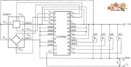
The voltage output angle detection circuit composed of the UZZ9000 and KMZ41 is shown as the chart, it uses a +5 V power supply, RP1 ~ RP2 are the offset voltage adjustment potentiometers, RP3 ~ RP4 are the gain adjustment potentiometers. The output end of R is the pull-down resistor. Output voltage can be sent to the digital voltmeter to show the measured angle values.
(View)
View full Circuit Diagram | Comments | Reading(649)
20 kbps light receiving circuit diagram
Published:2011/5/13 4:04:00 Author:Ecco | Keyword: 20 kbps light receiving

The circuit diagram uses optical transistor to drive three pieces of crystal amplifier tubes, generate TTL output, the data rate can reach 20,000 Kbp/s.
(View)
View full Circuit Diagram | Comments | Reading(1031)
Negative feedback ultra-linear amplifier circuit diagram
Published:2011/6/27 2:21:00 Author:Ecco | Keyword: Negative feedback, ultra-linear , amplifier
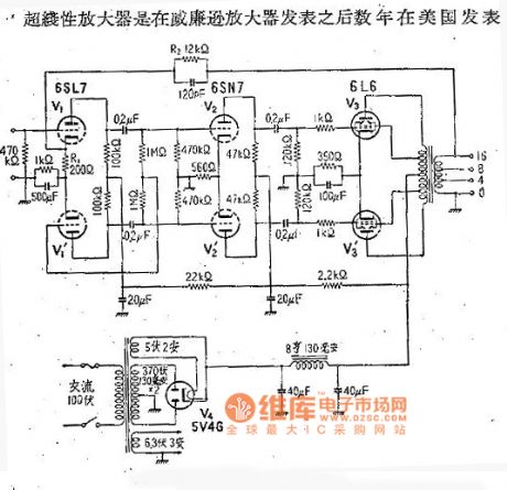
The ultra-linear amplifier is published after several years of Williamsonamplifier.
(View)
View full Circuit Diagram | Comments | Reading(1034)
Control double paper photosensitive circuit diagram
Published:2011/5/13 4:04:00 Author:Ecco | Keyword: Control double paper photosensitive

In the figure, the 6.3V and 2.5V of the transformer are served as light source for indicator light and spotlight electic bulb respectively. When the light of 3DU13 is resisted, the current can reach 8.5mA; When there's only one board to resist light , the current is 5~6mA, but at the same time, the relay still works; When there're two boards, the current is 3~4mA, the relay stops working. The mechanical action can drive 5kg iron absorption, and makes a control of a series of mechanical action, or connects to warning alarm.
(View)
View full Circuit Diagram | Comments | Reading(1269)
Switching circuit diagram with photocoupler
Published:2011/5/13 4:16:00 Author:Ecco | Keyword: Switching circuit, photocoupler

According to the figure 1, when the input signal ui is in low level, the transistor V1 is placed in a closed state, the current of LED in photocoupler B1 is nearly 0, the resistance between Q11 and Q12 is so high to result in the switch be off ; When the ui is in high level, the LED of Bi is lit, the resistance between Q11 and Q12 becomes low,the switchis switch on . As Ui is in low level, switch is impassable, the circuitry is in high level conducting state. In the same argument, in the figure 2, because of having no semaphore(Ui for low level), switch turns on, the circuitry is in low level conducting state.
(View)
View full Circuit Diagram | Comments | Reading(646)
Light gun circuit diagram
Published:2011/5/13 4:23:00 Author:Ecco | Keyword: Light gun

The light gunis used ascomputer handling, and it can orientate in the fluorescent screen of diaplay. When light gun receives the scanning signal from fluorescent screen, impulses light, then passes the control circuity, and the computer will show the location marked by light gun.To put a shadow shield with a window before light dependent resistor(LDR), when optical scanning electron beam makes the surface of fluorescent screen shine, the resistance value of LDR will shut down rapidly, T1, T2turn onand T3 discloses, the LED make LED turned off. That shows the light gun having indicated a word. And P1 is applied in adjusting the sensitivity of light gun.
(View)
View full Circuit Diagram | Comments | Reading(1626)
ULN2204,LN2204A,LN2204A 21 single chip audio integrated circuit
Published:2011/7/13 20:00:00 Author:leo | Keyword: Single chip, Audio, Integrated circuit

ULN204, ULN2204A and ULN2204A—21 are a kind of single chip audio integrated circuit used in pocket-sized radio and other kinds of radios.
1.ULN2204 integrated chip inner circuit diagram and pin functions:ULN2204 AM part contains AGC, MIX, LO, ZF and detecting circuit. The AM part does not include AGC and MIX circuit but only ZF and frequency discrimination circuit. Its pin functions are shown in the picture.
2.ULN2204 main parameters:The integrated circuit ULN2204 has a operating power supply voltage coverage of 3 V to 12 V with the classic voltage of 4.5 V.(1)When Ta is 25℃ and Vcc is 13V, the power consumption P(D) is 600 mW and current I(REY) is 60 mA.(2)Other main parameters are shown in the picture. (View)
View full Circuit Diagram | Comments | Reading(3708)
| Pages:1539/2234 At 2015211522152315241525152615271528152915301531153215331534153515361537153815391540Under 20 |
Circuit Categories
power supply circuit
Amplifier Circuit
Basic Circuit
LED and Light Circuit
Sensor Circuit
Signal Processing
Electrical Equipment Circuit
Control Circuit
Remote Control Circuit
A/D-D/A Converter Circuit
Audio Circuit
Measuring and Test Circuit
Communication Circuit
Computer-Related Circuit
555 Circuit
Automotive Circuit
Repairing Circuit