Basic Circuit
The typical application circuit of nRF401 single RF transceiver
Published:2011/6/23 2:55:00 Author:Ecco | Keyword: typical application circuit , single RF transceiver | From:SeekIC
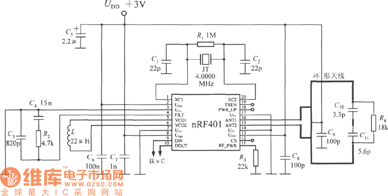
nRF401 typical application circuit is shown in the figure, UDD uses +3 V power supply. The R1, JT, C1 and C2 constitute the crystal oscillator circuit, C3, C4 and R2 form the loop filter. R3 is the power setting resistor. C5 is decoupling capacitors for power, C6 and C7 are de-noising capacitors. DIN, DOUT terminals are respectively connected to Microcontroller TXD (serial output), RXD (serial input) side. For simplifying the circuit, nRF401 and μC can be combined with a crystal oscillator circuit, the circuit is shown as below. X1, X2 are the crystal μC input and output, the oscillator frequency is directly added to the nRF401 end of XC2.
Reprinted Url Of This Article:
http://www.seekic.com/circuit_diagram/Basic_Circuit/The_typical_application_circuit_of_nRF401_single_RF_transceiver.html
Print this Page | Comments | Reading(3)

Article Categories
power supply circuit
Amplifier Circuit
Basic Circuit
LED and Light Circuit
Sensor Circuit
Signal Processing
Electrical Equipment Circuit
Control Circuit
Remote Control Circuit
A/D-D/A Converter Circuit
Audio Circuit
Measuring and Test Circuit
Communication Circuit
Computer-Related Circuit
555 Circuit
Automotive Circuit
Repairing Circuit
Code: