
Signal Processing
Index 65
FET_REGENERATIVE_DETECTOR
Published:2009/7/15 22:56:00 Author:Jessie
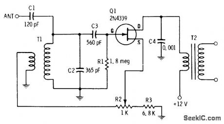
With 30-50 foot antenna wire, circuit gives sufficient volume for driving headphones connected to secondary of Lafayette AR-104 or equivalent audio driver transformer T2, for reception of broadcast stations when tuned over AM broadcast band with C2. Feedback control R2 is backed off slightly from point of oscillation, for maximum sensitivity in removing modulation from incoming carrier. When used for CW reception, circuit is left in oscillation and audible difference frequency is produced in output corresponding to marks and spaces. T1 is Miller 2004 or equivalent antenna transformer.-E. M. Noll, FET Principles, Experiments, and Projects, Howard W. Sams, Indianapolis, IN, 2nd Ed., 1975, p 235-237. (View)
View full Circuit Diagram | Comments | Reading(1203)
GATE_OPENING_100_KC_OSCILLATOR
Published:2009/7/15 21:50:00 Author:Jessie

Output voltages are taken across r-f chokes in collector circuits, for controlling number gates of crt display that creates handwritten numerals.-R L. White. Forming Handwritten like Digits on CRT display. Electronics,32:11,p138-140. (View)
View full Circuit Diagram | Comments | Reading(940)
VARIABLE_WIDTH_AND_DELAΥ
Published:2009/7/15 22:31:00 Author:Jessie
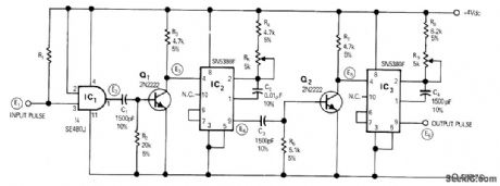
Produces variable-width blanking pulse at selectable delay time after triggering by input pulse. With values shown, output pulse range is 8 to 12 μs, and delay range is independently adjustable from 26 to 36 μs with R5.-D. E. Norris, Variable Delay Blanking-Pulse Generator, EDN|EEE Magazine, Dec. 1, 1971, p 49. (View)
View full Circuit Diagram | Comments | Reading(770)
SHORTENING_DUTY_CYCLE
Published:2009/7/15 22:30:00 Author:Jessie
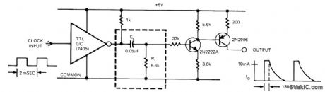
Clock-pulse differentiator/buffer shortens duty cycle of 500-Hz clock signal having positive period of 1000 ps. Open-collector 7405 inverter acts as buffer. Ct and Rt are primary differentiating components.Saturation of transistors provides some stretching of output and gives output pulse width of about 180 μs. Developed for driving regulated power supply having clock-controlled short-circuit protection.-J. L. Bohan, Clocking Scheme Improves Power Supply Short. Circuit Protection, EDN Magazine, Match 5, 1974, p 49-52.
(View)
View full Circuit Diagram | Comments | Reading(617)
MAX038_FUNCTION_GENERATOR_1
Published:2009/7/14 1:11:00 Author:May
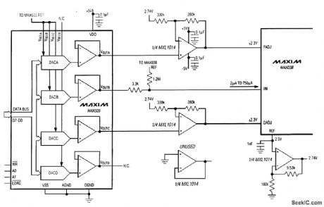
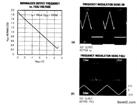
To adjust the frequency digitally, connect a voltage-output DAC to ⅡN via a series resistor, as shown. The converter output ranges from 0 V at zero to 2.5(255/256) V at full scale. Current injected by the converter into ⅡN, therefore, ranges from 0 to 748 μA. The 2.5-V reference and 1.2-Ω resistor inject a constant 2μA, so (by superposition) the net current into ⅡN ranges from 2 μA (at a code of 00000000) to 750μA (at 1111 1111). The quad DAC IC operates from 5 V or ±5 V. As described below, it can also provide digital control of FADJ and DADJ. For fine adjustments (±70 percent), apply a control voltage in the range ±2.3 V to the frequency adjust (FADJ) terminal. Both FADJ and ⅡN have wide bandwidths that allow the output frequency to be modulated at a maximum rate of about 2 MHz. As the more linear input, ⅡN is preferred for open-loop frequency use in a phase-locked loop. For digital control of FADJ, conftgure a DAC and external op amp (as shown in the figure) to produce an output ranging from -2.3 V (00000000) to 2.3 V (1111 1111). (View)
View full Circuit Diagram | Comments | Reading(962)
01_999_DUTY_CYCLE
Published:2009/7/15 22:28:00 Author:Jessie
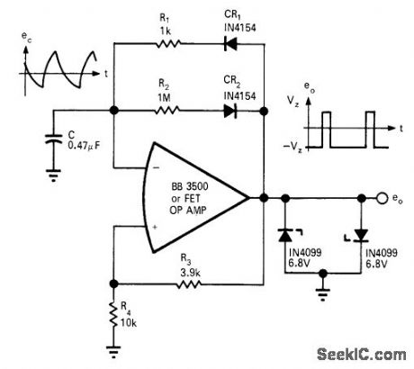
Single opamp circuit provides precise duty-cycle control of pulse train over wide dynamic range by choice of values for R1 and R2. Opamp forms gain element of astable MVBR, with pulse and space time intervals determined by feedback elements. Values shown give duty-cycle ratio of 0.001 and period of 1 s. J. Graeme, Pulse Generator Offers Wide Range of Duty Cycles, EDN|EEE Magazine, Sept.1, 1971, p 42-43. (View)
View full Circuit Diagram | Comments | Reading(916)
50_dB_ATTENUATION_CONTROL
Published:2009/7/15 23:27:00 Author:Jessie
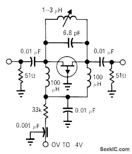
Low-cost FET in pi network serves as resistive attenuator providing up to 50-dB attenuation of 30-MHz level-controlled signal source by varying DC control voltage over range of 0 to 4 V. Tank circuit across source-drain leads of FET keeps phase shift under 2° over entire attenuation range. FET type is not critical -E. E. Baldwin, Voltage-Controlled Attenuator Has Minimum Phase Shift, EDN|EEE Magazine, Nov. 15, 1971, p 40. (View)
View full Circuit Diagram | Comments | Reading(776)
107_MHz_SWEEP_GENERATOR
Published:2009/7/14 0:35:00 Author:May
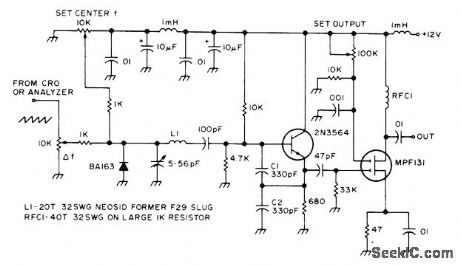
Can be used with CRO for studying response of IF amplifier or filter. Greater dynamic range is obtained by using with spectrum analyzer-Circuits, 73 Magazine, Holiday issue 1976, p 170. (View)
View full Circuit Diagram | Comments | Reading(0)
1000_V_PULSES
Published:2009/7/16 1:45:00 Author:Jessie

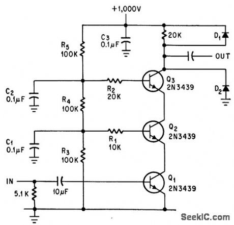
Positive 3-v input pulse switches Q1, Q2, and Q3 on in sequence, to produce l,000-v pulse with short rise time for driving 20-kv pulse tube. High-voltage rectifier diodes protect transistor string from spurious high-voltage spikes.-D. O. Hansen, Transistor Circuit Pulses l,000 Volts, Electronics, 38:18, p 86. (View)
View full Circuit Diagram | Comments | Reading(1038)
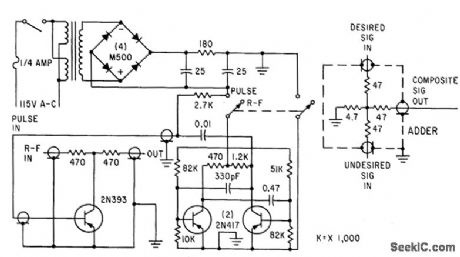
MARKER_GENERATOR
Published:2009/7/13 23:45:00 Author:May
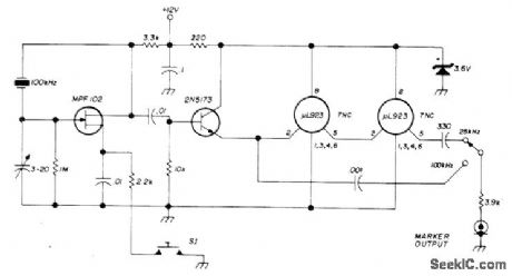
Crystal-controlled frequency marker for 80-meter SSB transceiver provides front-panel control of either 25-or 100-kHz markers. S1 activates circuit by completing source circuit of FET momentarily. Two μL923 JK flip-flops divide 100-kHz crystal frequency Down to 25 kHz 3-20 pF trimmer is adjusted to zero-beat crystal against receiver tuned to WWW.-D Hembling, Solid-State 80-Meter SSB Transceiver, Ham Radio, March 1973, p 6-17. (View)
View full Circuit Diagram | Comments | Reading(0)
AM_MIXER_IF_IC
Published:2009/7/16 1:37:00 Author:Jessie

Single National LM1820 chip provides all active stages for oscillator, mixer, IF amplifier, and AGC detector of superheterodyne AM broadcast radio. Omission of RF stage reduces cost at some sacrifice in sensitivity and stablity, along with more noise, but careful layout can minimize stability problems. Total gain is 88 dB. - Audio Handbook , National Semiconductor, Santa Clara, CA, 1977, p 3-4-3-8. (View)
View full Circuit Diagram | Comments | Reading(1042)
SIREN_GENERATOR
Published:2009/7/13 23:18:00 Author:May
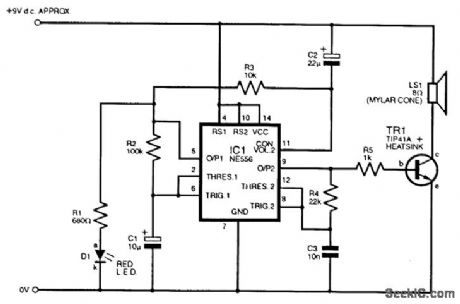
An adaptable siren generator circuit with a multitude of uses is shown. It is based around a 556 twin-timer chip, IC1. An audio tone is created by one timer section and is directly coupled to the driver transistor, TR1. The other half of the timer is used to modulate the frequency of the audio tone using the CONTROL VOLTAGE pin terminal of the audio-oscillator section, pin 11. If capacitor C2 is omitted from the circuit, a twin-tone alarm generator will be created. However, with C2 in place as shown, a wailing tone is produced. Capacitor C1 governs the rate of tone change and LED D1 flashes for extra effect. A waterproof Mylar-coned 8-Ω loudspeaker was used for LS1, and the volume can be adjusted for different impedances by altering the value of resistor R5. The circuit operates from approximately a 9-V rail. (View)
View full Circuit Diagram | Comments | Reading(2522)
NEGATIVE_RESISTANCE_DIODE
Published:2009/7/16 1:28:00 Author:Jessie
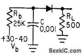
C discharges through negative-resistance diode and load after being charged by source, at rate determined by exponential function rather thon by RC time constant.-A. P. Schmid, Jr., Negative-Resistance Diode Handles High Power, Electronics, 34:34, p 44-46. (View)
View full Circuit Diagram | Comments | Reading(638)
CLASS_D_CB_NOISE_LIMITER
Published:2009/7/16 1:27:00 Author:Jessie

Two-step noise silencing system is almost essential for 27-Mc am receiver, because of ignition interference. large noise pulse swings plate of V3 negative and cuts off diode V3, to prevent noise pulse and audio signal from reaching volume control R3. Circuit recovers quickly, allowing audio signals to puss.-L. G.Sands, Citizens Radio Revision Spurs Equipment Design, Electronics, 32:15, p 55-57. (View)
View full Circuit Diagram | Comments | Reading(643)
SINE_SQUARE_WAVE_PHASE_SHIFT_OSCILLA_TOR
Published:2009/7/16 1:27:00 Author:Jessie

R1 controls oscillator frequency and R2 controls width of square wove having same frequency as sine-wave output.-F. W. Kear, Designing Transistor Phase-Shift Oscillators, Electronics, 35:11, p 72-74. (View)
View full Circuit Diagram | Comments | Reading(871)
AUDIO_DETECTOR_WITH_NOISE_LIMITER_2
Published:2009/7/16 1:26:00 Author:Jessie
Uses shunt limiter in conjunction with series limiter, so noise pulses are prevented from operating agc circuit and thus desensitizing i-f amplifier of communication receiver.Broad-band cathode follower is connected to output of diode detector.-NBS, Handbook Preferred Circuits Navy Aeronautical Electronic Equipment, Vol. 1, Electron Tube Circuits, 1963, p N12-1. (View)
View full Circuit Diagram | Comments | Reading(751)
3_V_BIPOLAR_LIMITER
Published:2009/7/16 1:25:00 Author:Jessie
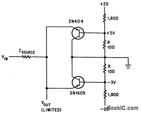
Upper transistor conducts when positive input pulse exceeds 3 v, and lower transistor shunts excess current to ground similarly for negative inputs above 3v, to keep output at 3 v for both polarities. Circuit provides own reference voltage.-S. B. Gray, Bipolar Limiter Reduces D-C Loss, Electronics, 38:24, p 65. (View)
View full Circuit Diagram | Comments | Reading(675)
IMPULSE_GENERATOR
Published:2009/7/16 1:25:00 Author:Jessie
Transistor electronic switch driven by. mvbr provides 10-microsec pulses at 1,500 pps for modulating receiver dose to 100% with pulsed interference.- B. T. Newman, Evaluating Radio Receiver Susceptibility to Interference, Electronics, 34:15, p 70-74. (View)
View full Circuit Diagram | Comments | Reading(953)
FAST_ACTING_LIMITER
Published:2009/7/16 1:24:00 Author:Jessie
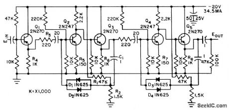
Provides compression of sine or square waves with minimum of phase distortion. Feedback paths in two direct-coupled transistor pairs improve limiting action of 100-kc pulse amplifier in which signals under 5 mv get 35 db of gain, with gain dropping to unity as signal strength increases to peak of 400 mv.-L. H. Dulberger, Pulse Amplifier with Nonlinear Feedback, Electronics, 31:45, p 86-87. (View)
View full Circuit Diagram | Comments | Reading(735)
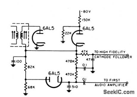
AUDIO_DETECTOR_WITH_NOISE_LIMITER_1
Published:2009/7/16 1:23:00 Author:Jessie

Uses conventional 6AL5 series noise limiter arrangement.-NBS, Handbook Preferred Circuits Navy Aeronautical Electronic Equipment, Vol. 1, Electron Tube Circuits, 1963, p N12-1. (View)
View full Circuit Diagram | Comments | Reading(772)
| Pages:65/195 At 206162636465666768697071727374757677787980Under 20 |
Circuit Categories
power supply circuit
Amplifier Circuit
Basic Circuit
LED and Light Circuit
Sensor Circuit
Signal Processing
Electrical Equipment Circuit
Control Circuit
Remote Control Circuit
A/D-D/A Converter Circuit
Audio Circuit
Measuring and Test Circuit
Communication Circuit
Computer-Related Circuit
555 Circuit
Automotive Circuit
Repairing Circuit