
Index 99
612AND_30_V_FOR_FM_TUNER
Published:2009/7/17 2:39:00 Author:Jessie

Provides regulated 30 V for voltage-controlled varicap tuning diodes, 12 V for other circuits of tuner, and optional 6 V for stereo decoder. Uses SGS IC regulators. - L. Nelson-Jones, F.M. Tuner Design-Two Years Later, Wireless World, June 1973, p 271-275. (View)
View full Circuit Diagram | Comments | Reading(796)
NE602_DC_BIAS_CIRCUIT
Published:2009/7/17 2:38:00 Author:Jessie

There are several ways to power the NE602. A resistor should be placed in series between the power supply and the NE602 (a and b).A zener diode (c) or a voltage regulator (d) can also be used. The resistor R1 should provide 4.5 to 8.0 V at pin 8 of the NE602. The current draw is about 2.4 to 2.8 mA. (View)
View full Circuit Diagram | Comments | Reading(775)
SIMPLE_MOBILE_RADIO_PROTECTOR
Published:2009/7/17 2:38:00 Author:Jessie

This circuit supplies power to a mobile radio only when the ignition is on and has a delay feature to prevent energizing the radio until the key has been on for several seconds, to avoid spikes and possible transients from the starter motor. (View)
View full Circuit Diagram | Comments | Reading(818)
3_260_MC_TUNNEL_DIODE_DIP_METER
Published:2009/7/17 2:38:00 Author:Jessie

Oscillator is tunable in six ranges, using plug-in circuits.-E, Gottlieb and J. Giorgis, Tunnel Diodes-Using Them as Sinusoidal Generators, Electronics, 36:2A, p 36-42. (View)
View full Circuit Diagram | Comments | Reading(664)
0_15_V_BENCH_SUPPLY
Published:2009/7/17 2:36:00 Author:Jessie
Provides up to 175 mA with ripple less than 1 mV. Choose Tr2 to handle load current. Current limiting is provided by 5.6-ohm (5R6) resistor and D1;when resistor drop exceeds about 1.2 V, current source Tr1 produces less current and output voltage is reduced.-J. A. Roberts, Bench Power Supply, Wireless World, May 1973, p 253. (View)
View full Circuit Diagram | Comments | Reading(880)
Bridge_linearization_function_circuit_using_an_AD534_multiplier_divider_chip
Published:2009/7/17 2:35:00 Author:Jessie
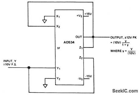
Bridge linearization function circuit using an AD534 multiplier/divider chip (courtesy Analog Devices, Inc.). (View)
View full Circuit Diagram | Comments | Reading(546)
AMPLIFIER_PROTECTOR
Published:2009/7/17 2:34:00 Author:Jessie
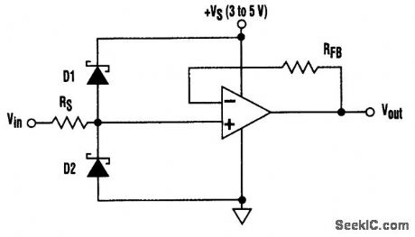
Unprotected amplifiers in noninverting, single-supply, voltage-follower stages might need external protection if input signals can exceed the rail voltages. Low-threshold Schottky diode clamps D1 and D2 provide safe clamping while RS limits the fault current. (View)
View full Circuit Diagram | Comments | Reading(865)
ELECTRONIC_CIRCUIT_BREAKER
Published:2009/7/17 2:33:00 Author:Jessie
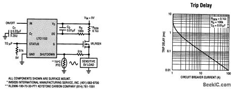
Fault conditions can quickly put stress on power sources and also on the loads themselves. Without a protective device to interrupt power during fault conditions, the supply can be overloaded or a load can overheat. The LTC1153 is a high-side MOSFET switch controller device with built-in circuit breaker, which turns off the MOSFET switch in the event of a fault. There is a built-in automatic reset, along with an input for thermal shutdown. The trip delay and reset times are fully adjustable. Because of its low (20 μA max) standby current, the LTC1153 can also be used in battery-powered equipment to protect the battery without reducing battery life. The switch can also be controlled with logic input. A status indicator reports fault conditions to a processor. (View)
View full Circuit Diagram | Comments | Reading(1146)
5_V_AT_2_A
Published:2009/7/17 2:33:00 Author:Jessie
Developed as supply for receiver frequency counter having LED display. FET having IDSS of about 7.5 mA serves in place of 1200-ohm resistor as current regulator. Power transformer is Triad F-26X with secondary rated 12.6 V center-tapped at 2.5 A.-H. H. Cross, The Chintzy 12, 73 Magazine, Feb. 1977, p 40-41. (View)
View full Circuit Diagram | Comments | Reading(638)
CATHODE_COUPLED_MAIN_GATE_MVBR_1
Published:2009/7/17 3:34:00 Author:Jessie
Provides positive unblanking gate. Used in radar to provide gate during which display sweep is generated. Capacitor switching provides choice of pate lengths.-NBS, Handbook Preferred Circuits Navy Aeronoutical Electronic Equipment, Vol. 1, Electron Tube Circuits, 1963, p N10-2. (View)
View full Circuit Diagram | Comments | Reading(568)
60_TO_72_MHz_VIDEO_AND_SOUND_RECEIVER_AND_IF_SYSTEM
Published:2009/7/17 3:34:00 Author:Jessie

This IF system uses a NE602 oscillator/mixer to convert VHF TV signals of 60 to 72 MHz (channe13 or channel4 under the U.S. NTSC) to 45 MHz. An SAW filter is used to provide bandpass filtering, followed by an LM1823 video IF/AGC/AFC/detector IC. Recovered video is fed to a sound trap and 4.5-MHz sound takeoff filter. Video is fed to the output emitter follower and is up to 1.5 V p-p into 75 Ω. An MC1357P FM IF/limiter/quadrature detector recovers audio information and provides 0.5 V p-p line-level audio. An LM555 oscillator and 1N914 diode act as a dc-to-dc converter system to derive a negative 3-V supply for the LM1823 AGC system. Both AFC and AGC voltages are available for interfacing with external down converters used for 440, 915, and 1280 MHz amateur TV reception. Operation is from a 12-V supply at about 200 mA.
A complete kit of parts, including PC board, is available from North Country Radio, P.O. Box 53, Wykagyl Station, New Rochelle, NY 10804-0053A. (View)
View full Circuit Diagram | Comments | Reading(2946)
UJT_BISTABLE_WITH_DIODE_DECOUPLING
Published:2009/7/17 3:33:00 Author:Jessie
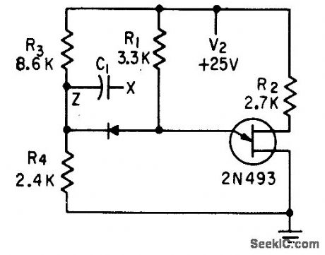
Needs only small negative trigger at X for turnoff.-T. P. Sylvan, Bistable Circuits Using Unijunction Transistors, Electronics, 31:51, p 89-91. (View)
View full Circuit Diagram | Comments | Reading(676)
Servo_motor_preamplifier_1
Published:2009/7/17 3:32:00 Author:Jessie


Servo motor preamplifier(courtesy Motorola Semiconductor Products Inc.). (View)
View full Circuit Diagram | Comments | Reading(702)
13_V_AT_2_A_WITH_NPN_TRANSISTORS
Published:2009/7/17 3:32:00 Author:Jessie
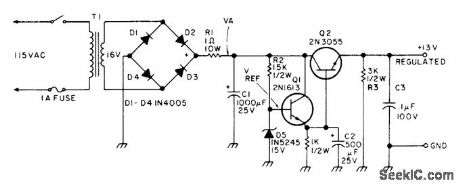
Q1 is reference voltage source and Q2 is series-pass regulator for basic supply suitable for running mobile FM transceiver or other 12-V portable equipment in home. Transformer secondary is 16-19 V, or can be 6-V and 12-V filament transformers in series. R1 protects rectifier diodes from surge current generated when supply is turned on. Article tells how to adapt circuit for other output voltages.-R. B. Joerger, Power Supply, 73 Magazine, Holiday issue 1976, p 40-41. (View)
View full Circuit Diagram | Comments | Reading(809)
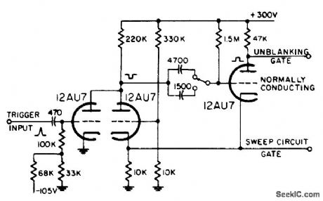
BISTABLE_MAIN_GATE_MVBR
Published:2009/7/17 3:32:00 Author:Jessie
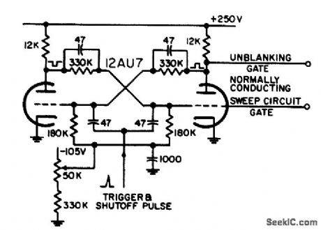
Provides positive unblanking gate. Used in radar to provide gates during which displayed sweep is generated, along with gates for waveforms that must be coincident with display sweep, but monostable mvbr is generally preferred for this application.-NBS, Handbook Preferred Circuits Navy Aeronautical Electronic Equipment, Vol. 1, Electron Tube Circuits, 1963, p N10-3. (View)
View full Circuit Diagram | Comments | Reading(591)
VARIABLE_VOLTAGE_REGULATOR
Published:2009/7/17 3:31:00 Author:Jessie

The op amp is wired as a×2 noninverting dc amplifier with a gam thatis determined by the R3/R2 ratio,The input voltage to the Op amp is variable between0 and 15 V via R5. The output voltage is therefore variable over the approximate range from 0.5 to 30 V The available output current has been boostedby adding transistor Q1 to the output. (View)
View full Circuit Diagram | Comments | Reading(0)
PROGRAMMABLE_ZENER
Published:2009/7/17 3:30:00 Author:Jessie
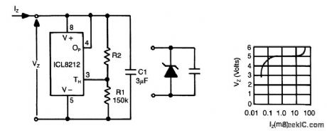
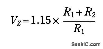
The ICL8212 is connected as a programmable zener diode,Zener voltages from 2 V up to 30 V can be programmed by suitably selecting R2.The zener voltage is∶
Because of the absence of internal compensation h the ICL8212,C1 is necessary to ensure stability.Two points worthy of note are the extremely low-knee current(less than 300 μA)and the low dynamic impedance (typically 4 to 7 ohms)over the operating current range of 300 μA to 12 mA. (View)
View full Circuit Diagram | Comments | Reading(1215)
REGULATOR_CIRCUIT
Published:2009/7/17 3:29:00 Author:Jessie
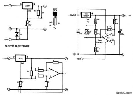
The special characteristic of this regulator is that the output voltage can be adjusted down to0 V. The regulation is provided by'an integrated regulator Type LM317. As is normal in supplies that can be adjusted to 0 V, this IC is used in conjunction with a zener diode. This diode provides a reference voltage that is equal, but of opposite sign, to the reference voltage (Ur) of the regulator, as shown in Fig. 74-1(a). Potential divider R1/R2 enables the output voltage to be adjusted.
In this circuit, the negative reference voltage is derived in a different manner: from the regulator with the aid of an op amp (Fig. 74-1(b)). The op amp is connected as a differential amplifier that measure, the voltage across R1 and inverts this voltage to Ur. An additional advantage of this method is that at low-output voltages, a change in the reference voltage has less effect on the output voltage than the circuit in Fig. 74-1(a). The prototype, constructed as shown in Fig. 74-1(c), gave very satisfactory results.
The op amp need not meet any special requirements: a μA741 works fine, although an LF356 gives a slightly better performance. The negative supply for the op amp can be obtained with the aid of a centertapped mains transformer. (View)
View full Circuit Diagram | Comments | Reading(746)
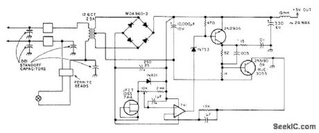
5_V_AND_±12_V
Published:2009/7/17 3:28:00 Author:Jessie
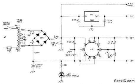
Also provides 18 unregulated for use with code regenerator driving automat Morse-code printer BR1 is Motorola MDA920-3 or HEP-R0802 bridge, LED is HP5082-4882 or HEP-P2000, U6 is LM341-5, MC7805, or HEP-C6110P. U7 is LM326H with TO5 finned clip-on heatsink, - H. Olson, CW Regenerator/Processor, 73 Magazine, July 1976, p 80-82. (View)
View full Circuit Diagram | Comments | Reading(1998)
Timer_one_shot_with_zero_standby_power
Published:2009/7/17 3:26:00 Author:Jessie
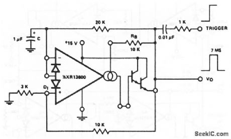
This circuit uses one section of an XR-13600 (Fig.11-1B) to form a timer or one-shot that draws no current from the supply until it is triggered. The trigger must be at least 2V, and the output is 7 ms with the values shown, EXAR Corporation Databook 1990 p 5-256 (View)
View full Circuit Diagram | Comments | Reading(552)
| Pages:99/291 At 2081828384858687888990919293949596979899100Under 20 |
Circuit Categories
power supply circuit
Amplifier Circuit
Basic Circuit
LED and Light Circuit
Sensor Circuit
Signal Processing
Electrical Equipment Circuit
Control Circuit
Remote Control Circuit
A/D-D/A Converter Circuit
Audio Circuit
Measuring and Test Circuit
Communication Circuit
Computer-Related Circuit
555 Circuit
Automotive Circuit
Repairing Circuit