
Index 59
Single Pulse Voltage Multiplier
Published:2013/1/25 1:19:00 Author:muriel | Keyword: Single , Pulse Voltage , Multiplier
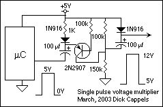
View full Circuit Diagram | Comments | Reading(518)
2X2 Mux
Published:2013/1/25 1:18:00 Author:muriel | Keyword: 2X2 Mux
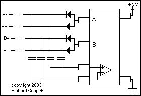
View full Circuit Diagram | Comments | Reading(862)
Four channel analog mux
Published:2013/1/25 1:18:00 Author:muriel | Keyword: Four channel, analog mux
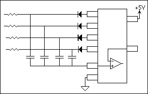
View full Circuit Diagram | Comments | Reading(489)
Two channel analog mux
Published:2013/1/25 1:17:00 Author:muriel | Keyword: Two channel , analog mux
View full Circuit Diagram | Comments | Reading(487)
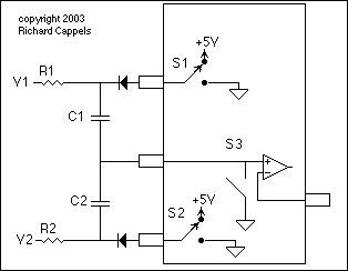
Various states of one channel
Published:2013/1/25 1:17:00 Author:muriel | Keyword: Various states, one channel
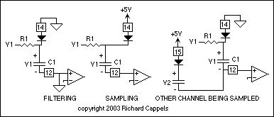
View full Circuit Diagram | Comments | Reading(407)
Bidirectional I/O pin
Published:2013/1/25 1:16:00 Author:muriel | Keyword: Bidirectional I/O pin
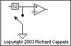
View full Circuit Diagram | Comments | Reading(397)
Five-use tri-state audio logic pen ( CD4066 , 555 )
Published:2013/1/24 1:43:00 Author:Ecco | Keyword: Five-use, tri-state , audio logic pen , 555
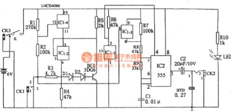
The circuit is mainly composed of multivibrator, four bidirectional switch CD4066 (IC1) and gate circuit with some resistive and capacitive components. The multivibrator 555 (IC2) consists of R7 , R8 , R9 and C1, and its oscillation frequency is affected by the off state of IC1-3.
(View)
View full Circuit Diagram | Comments | Reading(1291)
A simple second-tier logic state discriminator with 556
Published:2013/1/24 1:40:00 Author:Ecco | Keyword: simple, second-tier , logic state, discriminator , 556
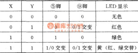
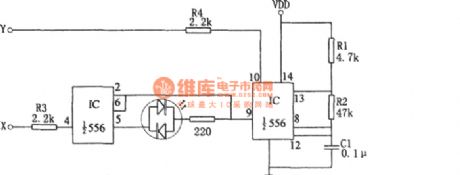
The relationship between light and logic state:
(View)
View full Circuit Diagram | Comments | Reading(573)
The external output analog voltage conversion circuit of DAC0832
Published:2013/1/23 2:29:00 Author:Ecco | Keyword: external output, analog voltage conversion
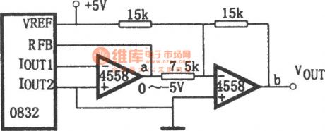
DAC0832 is a current output converter, if you need to get the analog voltage output, you must add an external converter circuit. The figure shows an analog voltage output circuit composed of two-stage operational amplifier. Unipolar analog voltage is output from the point a , and bipolar analog voltage is output from point b. If the reference voltage is +5 V, the point of a outputs 0 -5V voltage, and point b outputs ± 5V voltage.
(View)
View full Circuit Diagram | Comments | Reading(1274)
The connection method of AD7520 basic circuit
Published:2013/1/23 2:33:00 Author:Ecco | Keyword: connection method , basic circuit
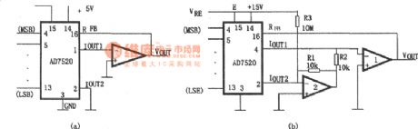
The AD7520 is an inexpensive, medium - resolution D / A converter chip, and it is composed of CMOS current switch and T resistor network, it has a simple structure, flexible configuration and good versatility. The connection method of the AD7520 basic circuit is shown as figure, wherein the figure (a) is a unipolar output basic conversion circuit; Figure (b) is the basic conversion circuit of the bipolar output.
(View)
View full Circuit Diagram | Comments | Reading(750)
Analog regulator
Published:2013/1/22 21:22:00 Author:muriel | Keyword: Analog regulator

View full Circuit Diagram | Comments | Reading(651)
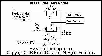
Switchable Reference Impedance
Published:2013/1/22 21:13:00 Author:muriel | Keyword: Switchable Reference Impedance
View full Circuit Diagram | Comments | Reading(520)
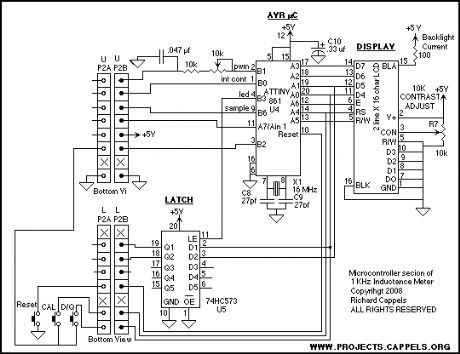
Micro controller, User Interface, and Display
Published:2013/1/22 21:10:00 Author:muriel | Keyword: Micro controller, User Interface, Display
View full Circuit Diagram | Comments | Reading(623)
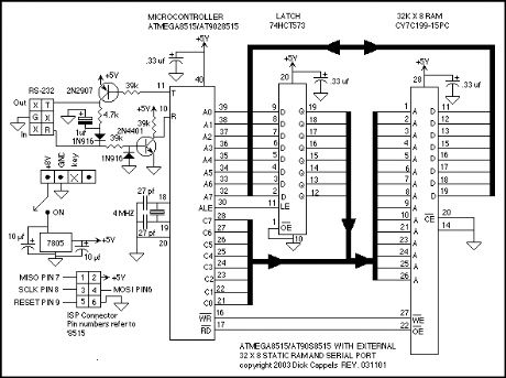
ATTOBASIC WITH 32K OF EXTERNAL RAM
Published:2013/1/22 20:53:00 Author:muriel | Keyword: ATTOBASIC, 32K, EXTERNAL RAM
View full Circuit Diagram | Comments | Reading(890)
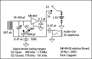
MK-484 Evaluation Board
Published:2013/1/22 20:52:00 Author:muriel | Keyword: MK-484 , Evaluation Board
View full Circuit Diagram | Comments | Reading(799)
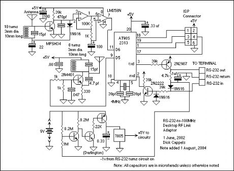
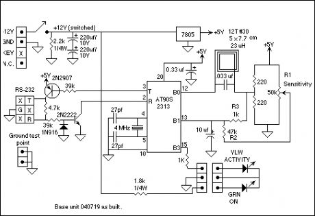
RS-232 to 100 MHz RF desktop channel adapter
Published:2013/1/22 20:48:00 Author:muriel | Keyword: RS-232, 100 MHz , RF , desktop, channel adapter
View full Circuit Diagram | Comments | Reading(583)
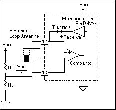
Tiny Tuned Loop Antennas
Published:2013/1/22 20:47:00 Author:muriel | Keyword: Tiny Tuned, Loop Antennas
View full Circuit Diagram | Comments | Reading(531)
Minimum Mass Wireless Coupler Terminal Interface
Published:2013/1/22 20:45:00 Author:muriel | Keyword: Minimum Mass , Wireless Coupler, Terminal Interface
View full Circuit Diagram | Comments | Reading(590)
Minimum Mass Wireless Coupler
Published:2013/1/22 20:43:00 Author:muriel | Keyword: Minimum Mass, Wireless Coupler
View full Circuit Diagram | Comments | Reading(585)
VFC121V / F converter application temperature measurement system
Published:2013/1/22 2:40:00 Author:Ecco | Keyword: converter application , temperature measurement system
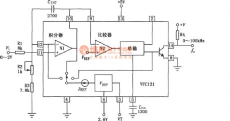
VFC121 uses high-frequency NPN / PNP charge balance technology to realize V / F conversion, and its power supply is flexible( 4.5 to 36V), and the voltage output is proportional to absolute temperature, thus it can be used as the system environment temperature measurement for D / A converters, data acquisition and system deviating occasion. VFCl21 uses 0IP 14-pin double-row arrangement package, and its pinout and internal circuit block diagram is shown as below.
(View)
View full Circuit Diagram | Comments | Reading(1004)
| Pages:59/471 At 204142434445464748495051525354555657585960Under 20 |
Circuit Categories
power supply circuit
Amplifier Circuit
Basic Circuit
LED and Light Circuit
Sensor Circuit
Signal Processing
Electrical Equipment Circuit
Control Circuit
Remote Control Circuit
A/D-D/A Converter Circuit
Audio Circuit
Measuring and Test Circuit
Communication Circuit
Computer-Related Circuit
555 Circuit
Automotive Circuit
Repairing Circuit