
Index 309
Automatic_reset
Published:2009/7/24 12:16:00 Author:Jessie
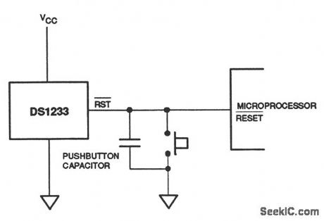
This circuit shows a DS1233 EconoReset chip that is used to monitor the power supply of a processor-based system and to provide automatic reset. The DS1233 contains a precision temperature-compensated reference and comparator circuit that is used to monitor the power-supply (VCC) status. When an out-of-tolerance condition is detected, RST becomes active, and shuts off the processor. When VCC returns to an in-tolerance condition, RST is kept in the active state for about 350 ms to allow the power supply and processor to stabilize. The DS1233 also debounces a pushbutton closure (when used), and generates a 350-ms reset pulse upon release. Notice that when an external pushbutton is used, a capacitor between 100 pF and 0.01μF must be connected between RST and ground. Where additional reset current is required, a minimum capacitance of 500 pF should be used, along with a parallel external pull-up 1-kΩ resistor (minimum). Dallas Semiconductors, Product Data Book, 1992/1993, p. 10-59. (View)
View full Circuit Diagram | Comments | Reading(692)
Low_power_micromonitor_with_pushbutton_and_watchdog_timer
Published:2009/7/24 12:13:00 Author:Jessie
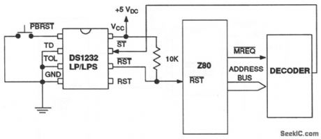
This circuit is similar to that of Fig. 6-50, but with the addition of a watchdog-timer function to monitor software execution. The timer function forces RST and RST signals to the active state (shutting down the processor) when the ST input is not stimulated for a predetermined time period (because of some failure in software execution). The time period is set by the TD input to be about 150 ms with TD connected to ground, 600 ms with TD left unconnected, and 1.2 s with TD connected to VCC . The timer starts timing out from the set-time period as soon as reset signals are inactive. The ST input can be taken from address, data and/or control signals. When the processor is executing software, these signals are present, which causes the watchdog to be reset prior to time-out. Dallas Semiconductors, Product Data Book, 1992/1993, p. 10-54. (View)
View full Circuit Diagram | Comments | Reading(675)
Low_power_micromonitor_with_pushbutton
Published:2009/7/24 12:09:00 Author:Jessie
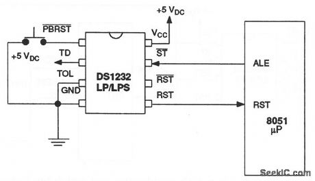
This circuit shows a DS1232LP/LPS used to monitor and control the power supply and software execution of a processor-based system, and to provide a pushbutton reset. When VCC falls below a preset level (as defined by the TOL pin connection) the DS1232 outputs RST and RST reset signals. With TOL connected to ground, reset becomes active as VCC falls below 4.75 V. When TOL is connected to VCC, reset becomes active as VCC falls below 4.5 V. On power-up, RST and RST are kept active for a minimum of 250 ms to allow the power supply and processor to stabilize. The pushbutton reset input PBRST requires an active low. Internally, this input is debounced and timed so that reset signals of at least 250 ms (minimum) are generated. The 250-ms delay starts as the pushbutton reset input is released from low level. Dallas Semiconductors, Product Data Book, 1992/1993, p. 10-54. (View)
View full Circuit Diagram | Comments | Reading(702)
Digital_power_monitor_that_operates_from_the_power_line
Published:2009/7/24 12:05:00 Author:Jessie
This circuit is similar to that of Fig. 6-47, except that the voltage sense point is taken directly from the ac power line, instead of from the power supply, and an optoisolator (chapter 9) is used between the line and DS1231. Dallas Semiconductors, Product Data Book, 1992/1993, p. 10-42. (View)
View full Circuit Diagram | Comments | Reading(491)
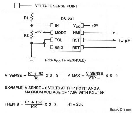
Digital_power_monitor_with_line_isolation
Published:2009/7/24 12:04:00 Author:Jessie
This circuit is similar to that of Fig. 6-47, except that an optoisolator (chapter 9) is used between the voltage sense point and the DS1231 to provide line isolation. Dallas Semiconductors, Product Data Book, 1992/1993, p. 10-41. (View)
View full Circuit Diagram | Comments | Reading(658)
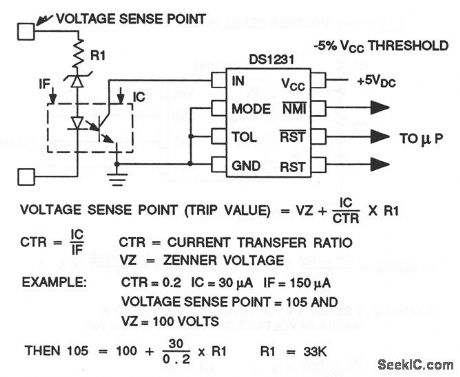
Digital_power_monitor
Published:2009/7/24 12:03:00 Author:Jessie
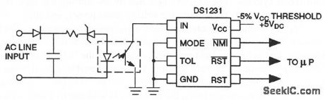
This circuit shows a DS1231 power monitor chip that is used to control a digital-system power supply. The DS1231 uses a temperature-compensated reference circuit to provide both an orderly shutdown and automatic restart of processor-based systems. The DS1231 operates by monitoring the high-voltage inputs to the power-supply regulators (at a voltage sense point), and applying RST or RST and NMI (nonmaskable interrupt) control signals to the processor. The time for processor shutdown is directly proportional to the available hold-up time of the power supply. Just before the hold-up time is exhausted, the DS1231 unconditionally halts the processor (to prevent spurious cycles) by enabling reset when VCC falls below a selectable 5 or 10% threshold. Notice that the TOL pin is grounded for a 5% threshold. When power returns, the processor is held inactive until well after power conditions have stabilized, safeguarding any nonvolatile memory in the system from inadvertent data changes. Dallas Semiconductors, Product Data Book, 1992/1993, p. 10-40. (View)
View full Circuit Diagram | Comments | Reading(759)
RS_232_transmitter_receiver_with_external_power
Published:2009/7/24 11:59:00 Author:Jessie
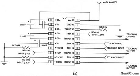
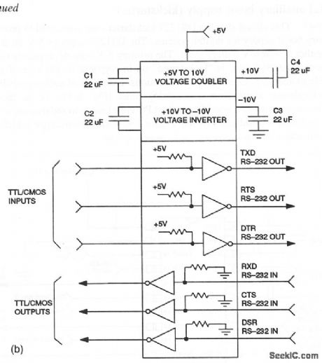
This circuit shows a DS1229 that is connected as a triple RS-232 transmitter/receiver. The DS1229 has two internal charge pumps that are used to generate ±10 V, and six level translators. Three of the translators are RS-232 that convert TTL/CMOS inputs into +9-V RS-232 outputs. The other three translators are RS-232 receivers that convert RS-232 inputs to 5-V TTL/CMOS outputs. Figurd 6-46B shows some typical RS-232 interconnections. Dallas Semiconductors, Product Data Book, 1992/1993, p. 10-33, 10-34. (View)
View full Circuit Diagram | Comments | Reading(639)
Digital_auxiliary_boost_supply_kickstarter
Published:2009/7/24 11:56:00 Author:Jessie
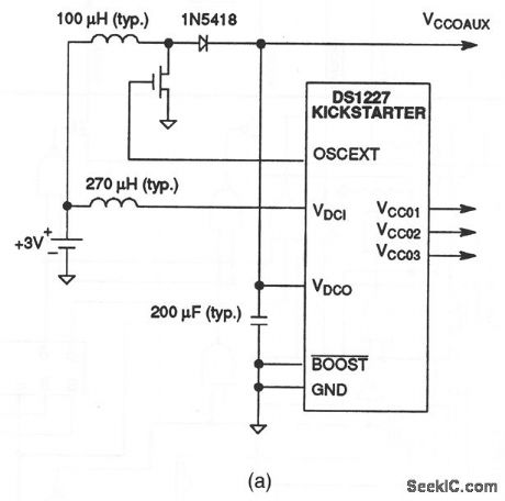
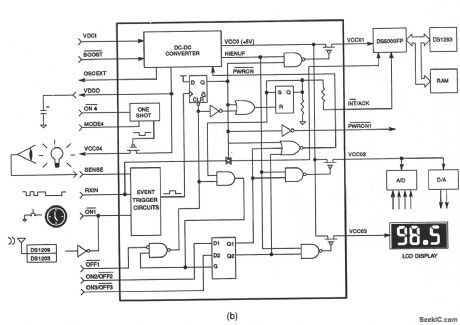
This circuit shows a DS1227 kickstarter chip connected to provide an auxiliary boost supply for digital systems. The DS1227 supplies 5 V on demand from either a 3- or 6-V battery input. The primary 5-V outputs, typically tied to a microcontroller VCC pin, is kickstarted on in response to any one of several possible momentary, external signal transitions. Examples of such signals include a clock/calendar alarm from a watchdog timer (Fig. 6-51), or an incoming asynchronous serial-data word from a host PC via a line-powered transceiver (Fig. 6-60), or a simple pushbutton switch. Figure 6-45B shows some typical kickstarter interconnections. Dallas Semiconductors, Product Data Book, 1992/1993, p. 10-17, 10-21. (View)
View full Circuit Diagram | Comments | Reading(525)
Serial_DRAM_nonvolatizer
Published:2009/7/24 11:51:00 Author:Jessie
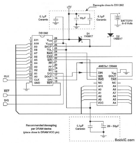
This circuit shows a DS1262 Serial DRAM nonvolatizer chip that is used to enable read/write access of DRAM from a simple 3-wire serial port. Refresh and RAS/CAS timing for the DRAM are performed automatically, transparent to operation of the serial port. In addition, the DS1262 performs all power switching and refresh duties that are necessary to retain DRAM data when the primary power supply fails. The backup supply input accepts a wide voltage range, suitable for use with rechargeable batteries. The DS1262 also provides an electronic gas gauge that can predict the condition of the backup supply. When the VCC1 power begins to drop, an internal circuit senses the changes, and the data-retention mode begins. The VCC1 input is then disconnected from the VCC0 output and the backup supply connected to the BKUP pin is switched in. The DS1262 also monitors the backup supply condition. If the backup supply is below VCC1, the backup-condition output pinBC is driven active low, and remains in this state until the backup supply voltage is restored to a level above VCC1. Dallas Semiconductors, Product Data Book, 1992/1993, p. 9-59. (View)
View full Circuit Diagram | Comments | Reading(1538)
TTL_DTL_interface_to_telephone_equipment
Published:2009/7/24 11:46:00 Author:Jessie
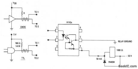
This circuit provides interface of positive-logic circuits to negative-powered telephone equipment. In addition, the circuit provides for a change in voltage level (+5 and -50 V), as well as isolation, using an H11G optoisolator. Motorola Thyristor Device Data, 1989, p. 6-54. (View)
View full Circuit Diagram | Comments | Reading(515)
A_MUX_with_16_bit_serial_interface
Published:2009/7/24 10:48:00 Author:Jessie
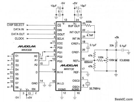
In this circuit, a 16-bit MAX132 A/D provides a serial interface for a MAX328 MUX, with both serial data input and output. The A/D is a 16-bit modified dual-slope converter. In addition to the main 16-bit output, the A/D also provides 3 guard-band bits with add resolution in the A/D noise region, but it can raise resolution if software averaging is used. The MAX328 MUX is addressed through four programmable bits PG0-PG3, which are sot through the MAX132 serial input. Maxim, 1992,Appications and Product Highlights, p. 8-4. (View)
View full Circuit Diagram | Comments | Reading(1598)
DIVIDING_ANALOG_VOLTAGES
Published:2009/6/30 21:19:00 Author:May
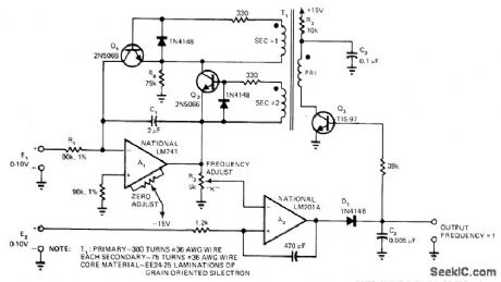
Charge-and-dump V/F conversion technique is used to obtain quotient of two analog voltages digitally. Applications include measurement of total mass flow of gas under constant pressure. With Q1 and Q2 normally off, C1 charges at rate proportional to input E1, producing negative ramp at output of integrating opamp A1. When R2 wiper voltage exceeds E2, output of A2 goes high, tuming on Q3 and temporarily driving Q1 and Q2 into conduction. This process discharges C1, resetting output of A1 to zero. With values shown, E1 and E2 equal, and wiper of R2 at midpoint, circuit output is 10,000 pulses per hour, suitable for driving electromechanical counter. Output frequency is proportional to average DC value of E1 even when input changes rapidly.—H. L. Trietley, Voltage-to-Frequency Converter Performs Division, EDN Magazine, Jan. 5, 1978, p 79-80. (View)
View full Circuit Diagram | Comments | Reading(569)
VOLTAGE_TO_PULSE_WIDTH
Published:2009/6/30 21:16:00 Author:May
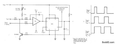
Opamp and timer together convert input voltage level to width of output pulsewith accuracy better than 1%. Output is at same frequency as input.— Signetics Analog Data Manual, Signetics Sunnyvale, CA, 1977, p 726-727. (View)
View full Circuit Diagram | Comments | Reading(703)
GRAY_TO_BINARY
Published:2009/6/30 21:15:00 Author:May

Convelts first 4 bits of Gray-code word to binary output. Uses two MC7496 shift registers and logic elements to transfer data serially from input register through MC1812 EXCLUSIVE-ORIC to output register. One requirement is that strobe on pin 8 of input register must complete its function before clock appears on pin 1 of register. When this and other timing conditions are satisfied, converter will work at speeds up to about 10 megabits per second.—J. Barnes, Analog-to-Digital Cyclic Converter, Motorola, Phoenix, AZ, 1974, AN-557, p 9. (View)
View full Circuit Diagram | Comments | Reading(2256)
VOLTAGE_TO_FREQUENCY
Published:2009/6/30 21:11:00 Author:May
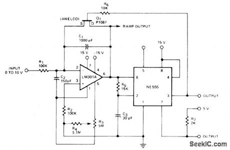
Input voltage range of 0 to -10 VDC is converted by opamp and timer to proportional frequency with good linearity. Circuitis TTL-compatible, Accuracy is 0.2%.— Signetics Analog Data Manual, Signetics, Sunnyvale, CA, 1977, p 727-729. (View)
View full Circuit Diagram | Comments | Reading(571)
ULTRASONIC_PEST_REPELLER_1
Published:2009/6/30 21:05:00 Author:May
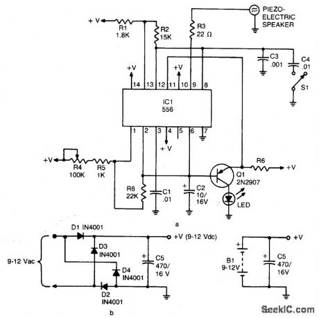
The device emits ultrasonic sound waves that sweep between 65,000 and 25,000 hertz. Designed around a 556 dual timer, one half operated as an astable )nultivibrator with an adjustable frequency of 1 to 3 Hz. The second half is also operated as an astable multivibrator but with a fixed free running frequency around 45,000 Hz. The 25-65 kHz sweep is ac-complished by coupling the voltage across C2 (the timing capacitor for the first half of the 556) via Q1 to the control voltage terminal (pin 11) of the second half of the 556. The device that radiates the ultrasonic sound is a piezo tweeter. (View)
View full Circuit Diagram | Comments | Reading(1123)
A_D_converter_for_3_digit_LCD_display
Published:2009/7/24 9:57:00 Author:Jessie
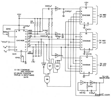
This circuit shows a CA3162E and three CD4056B LCD decoder/drivers connected in a typical LCD application. With pin 6 of the CA3162E floating (as shown), the sampling rate is 4 Hz. The negative sign (-) is decoded as a negative sign (-), and the positive overload indicator (E) as an H . To adjust, short terminals 10 and 11 of the CA3162E, and adjust the zero control for a reading of 000 on the display. Then, apply 900 mV at terminals 10 and 11, and adjust the gain control for a reading of 900 on the display. Harris Semiconductors, Data Acquisition, 1991, p. 2-5. (View)
View full Circuit Diagram | Comments | Reading(1838)
Differential_line_driver_to_drive_an_ARINC_429_bus
Published:2009/7/24 9:52:00 Author:Jessie
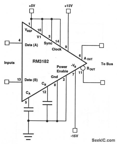
With this circuit, the output impedance is 75Ω. When data-A is high and data-B is low, AOUT swings to +VREF and BOUT swings to -VREF, and vice versa. The slew rate is set by CA/CB. Typical values are 15 pF for 100 Kb/s and 500pF for 12.5 to 14 Kb/s. Raytheon Linear Integrated Circuits, 1989, p. 11-6. (View)
View full Circuit Diagram | Comments | Reading(645)
PHOTOELECTRIC_SMOKE_DETECTOR_NON-LATCHING
Published:2009/6/30 3:48:00 Author:May
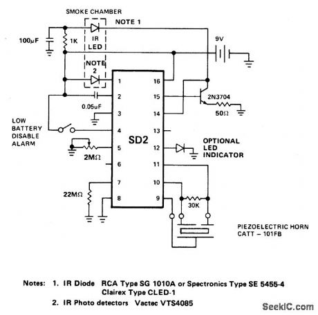
The LED predriver output pulses an ex-temal transistor which in turn, switches on the infrared light emitting diode at a very low duty cycle. The desired IR LED pulse period is determined by the value of the external timing resistor. The Smoke Sensitivity is adjustable through a trimmer resistor which varies the IR LED pulse width. The light sensing element is a silicon photovoltaic cell which is held at near zero bias to minimize leakage currents. The circuit can detect signals as low as 1 mV and generate an alarm. The IR LED pulse repetition rate increases when smoke is detected. (View)
View full Circuit Diagram | Comments | Reading(662)
A_D_converter_with_latch
Published:2009/7/24 9:49:00 Author:Jessie
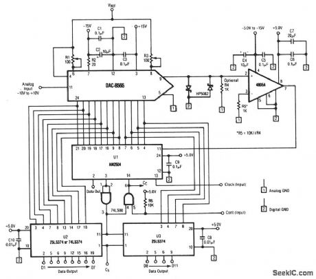
This circuit shows a DAC and comparator that is used with an SAR form a 12-bit A/D converte. Latched output is provided by the 25LS374.The reference is set by R1 and the bipolar offset is controlled by R3. Raytheon Linear Integrated Circuits, 1989, p. 6-96. (View)
View full Circuit Diagram | Comments | Reading(1007)
| Pages:309/471 At 20301302303304305306307308309310311312313314315316317318319320Under 20 |
Circuit Categories
power supply circuit
Amplifier Circuit
Basic Circuit
LED and Light Circuit
Sensor Circuit
Signal Processing
Electrical Equipment Circuit
Control Circuit
Remote Control Circuit
A/D-D/A Converter Circuit
Audio Circuit
Measuring and Test Circuit
Communication Circuit
Computer-Related Circuit
555 Circuit
Automotive Circuit
Repairing Circuit