
Index 305
MEASURING_PHASE_DIFFERENCE_FROM_0°to±180°
Published:2009/7/1 2:15:00 Author:May

This method is capable of measuring phase between 0 to ±180°. The generated square waves A and B are fed to a D flip-flop which gives an output C equal to logic 1 when input 1 leads input 2 and equal to logic 0 in case of lagging. When C = logic 0, the output of the amplifier F will be positive proportional to the average value E of the output of the EX-OR. When C = logic 1, F will be negative and also proportional to E by the same factor. Hence, the output of the meter is positive in case of lagging and negative for leading. The circuit is tested for sinusoidal inputs and indicates a linearity within l%. Measurements are unaffected by the frequency of the inputs up to 75 kHz. (View)
View full Circuit Diagram | Comments | Reading(945)
AC_DC_CLOCK
Published:2009/7/1 2:14:00 Author:May

When AC power fails, MCD-2 optoisolator senses voltage drop and makes Schmitt trigger force strobe input of clock chip to ground, blanking display and reducing current P' ain from 2O0 mA on AC to 12 mA on 9-V standby battery. Clock will run for days on 1000-mAh battery. Two LED pairs that form colons between time dighs are operated from digit strobe Iines and remain lit when display is blanked, but draw only 1 mA.-S. l. Green, Dig-ital Clock Keeps Counting Even When AC Power Fails, EDN Magazine, Dec, 20, 1974, p 49-51. (View)
View full Circuit Diagram | Comments | Reading(1224)
WIRE_TRACER
Published:2009/7/1 2:14:00 Author:May

The tracer detects the weak magnetic field of any current-carrying house wiring and amplifies this signal to a level that is adequate for driving a magnetic earpiece. The unit uses a telephone pick-up coil to detect the magnetic field. (View)
View full Circuit Diagram | Comments | Reading(3968)
STANDBY_SUPPLY
Published:2009/7/1 2:10:00 Author:May

Phase-shift oscillator Ql operates from AC line through bridge-rectifier power supply and provides line-synchronized 60-Hz power to standard digital clock through isolating emitter-follower Q2. Curing power outage, oscillator is switched automatically to battery by diode network and provides reason-ably accurate signal for operating clock. Free-running oscillator is adjusted to be slightly Iow, such as 59.9 Hz. For reasonably Iong power outage, say 4 h, this 0.1-Hz error is equivalent to 0.167% error in time, so clock loses only 24 s during outage. C1 and C2 are 200 to 300 μF. Ad-just R1 to give output just below 60 Hz on battery operation. To minimize battery drain, LEDs on digital clock are not energized during standby.-R. S. Isenson, Digital Clock Fail-Safe, 73 Magazine, July 1977, p 168-169. (View)
View full Circuit Diagram | Comments | Reading(653)
MAGNETOMETER
Published:2009/7/1 2:08:00 Author:May

The circuit uses two general-purpose npn transistors, Q1 and Q2, and a special hand-wound, dual-coil probe ferrets out the magnetism. Q1 and its associated components form a simple VLF oscillator circuit, with L1, C2, and C3 setting the frequency. The VLF signal received by the pickup coil, L2, is passed through C5 and rectified by diodes Dl and D2. The small dc signal output from the rectifier is fed to the base of Q2 (conftgured as an emitter follower), which is then fed to a 0-1 mA meter, M1. (View)
View full Circuit Diagram | Comments | Reading(5842)
VOLTAGE_REFERENCE_1
Published:2009/7/1 2:08:00 Author:May

View full Circuit Diagram | Comments | Reading(489)
BIPOLAR_DC_DC_CONVERTER_REQUIRES_NO_INDUCTOR
Published:2009/7/1 2:08:00 Author:May


Inverters Ula and Ulb form a 20-kilohertz oscillator whose square wave output-further shaped by D2, R4, and R5 and by D3, R6, and R7-drives power field-effect transistors Q2 and Q3. The p-channel and n-channel FETs conduct alternately, in a push-pull configuration. When Q2 conducts, the positive charge on Cout forces diode D4 to conduct as well, which produces a positive voltage, determined by zener diode D5, at terminal A. Similarly, when Q3, in its turn conducts, the negative charge on Cout forces D7 to do so as well. A negative voltage, therefore, develops at terminal B, whose level is set by D6. (View)
View full Circuit Diagram | Comments | Reading(1022)
VOLTAGE_REFERENCE
Published:2009/7/1 2:08:00 Author:May

View full Circuit Diagram | Comments | Reading(1069)
Digital_memory_backup_for_SRAMs
Published:2009/7/24 12:26:00 Author:Jessie

This circuit shows a DS1236 that is used to control battery-backup operation for a static RAM. First, the DS1236 contains a switch to direct SRAM power from the 5-V supply (VCC) or from an external battery (VBAT), whichever is greater. The switched supply (VCCO) can also be used to battery-back a CMOS processor. Second, the same power-fail detection (using RST and RST ) that is described for the digital power monitor (Fig. 6-53) is used to hold the chip-enable output (CEO ) to within 0.3 V of VCC or to within 0.7 V of VBAT. This write-protection mechanism occurs as VCC falls below a specified trip point, VCCTP. Dallas Semiconductors, Product Data Book, 1992/1993, p. 10-74. (View)
View full Circuit Diagram | Comments | Reading(2164)
FREQUENCY_DIVIDER
Published:2009/7/1 1:46:00 Author:May
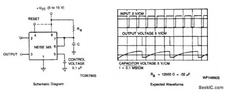
If the input frequency is known, the timer can easily be used as a frequency divider by adjusting the length of the timeing cycle. Figure shows the waveforms of the timer when used as a divide-by-three circuit. This application makes use of the fact that this circuit cannot be retriggered during the timing cycle. (View)
View full Circuit Diagram | Comments | Reading(1940)
PHOTOCURRENT_INTEGRATOR
Published:2009/7/1 1:44:00 Author:May
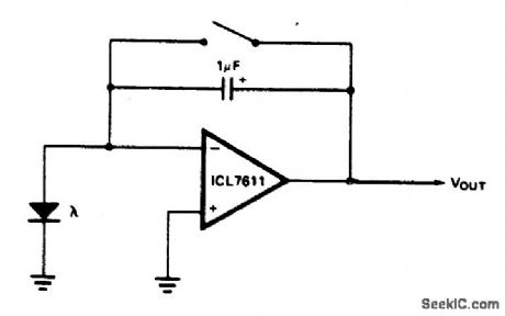
Low leakage currents allow integration times up to several hours. (View)
View full Circuit Diagram | Comments | Reading(405)
LOW_FREQUENCY_DIVIDER
Published:2009/7/1 1:41:00 Author:May
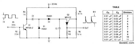

The ratio of capacitors C1 and C2 determines division. With a positive pulse applied to the base of Q1, assume that C1 = C2 and that C1 and C2 are discharged. When Q1 turns off, both C1 and C2 charge to 10 volts each through R3. On the next pulse to the base of Q1, C1 is again discharged but C2 remains charged to 10 volts. As Q1 turns off this time, C1 and C2 again charge. This time C2 charges to the peak point firing voltage of the PUT causing it to fire. This discharges capacitor C2 and allows capacitor C1 to charge to the line voltage. As soon as C2 discharges and C1 charges, the PUT turns off. The next cycle begins with another positive pulse on the base of Q1 which again discharges C1. The input and output frequency can be approximated by the equationFor a 10 kHz input frequency with an amplitude of 3 volts, the table shows the values for C1 and C2 needed to divide by 2 to 11. (View)
View full Circuit Diagram | Comments | Reading(1306)
FAST_BLINKER
Published:2009/7/1 1:40:00 Author:May
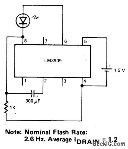
View full Circuit Diagram | Comments | Reading(428)
FREQUENCY_DOUBLER_WORKS_TO_1_MHz
Published:2009/7/1 1:37:00 Author:May
Adding components Q3, D3, and resistors R3 through R6 to a conventional complementary symmetry class AB buffer can double the frequency of an input sine wave. (View)
View full Circuit Diagram | Comments | Reading(646)
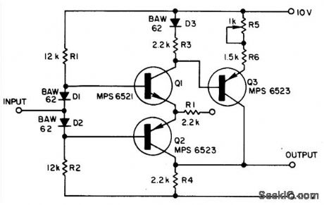
NONSELECTIVE_FREQUENCY_TRIPLER_USES_TRANSISTOR_SATURATION_CHARACTERISTICS
Published:2009/7/1 1:34:00 Author:May
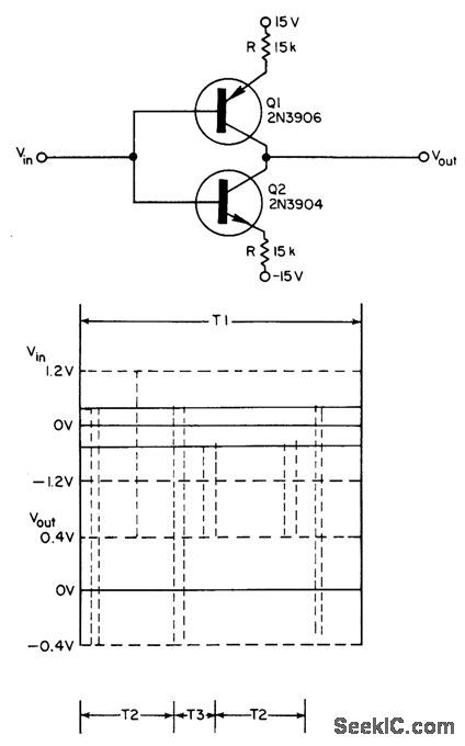
The turn-on and turn-off characteristics of two complementary transistors can be combined to attain nonselective frequency tripling. The resulting circuit handles any periodic waveform with nonvertical sides. Each input signal peak produces three output signal peaks. The additional peaks occur where the input signal causes saturation of one of the two transistors.The circuit operates over a frequency range from dc to the upper limits of the comple-mentary transistor pair. About the only disadvantage of the circuit is the lack of symmetry of the output signal peaks. (View)
View full Circuit Diagram | Comments | Reading(1127)
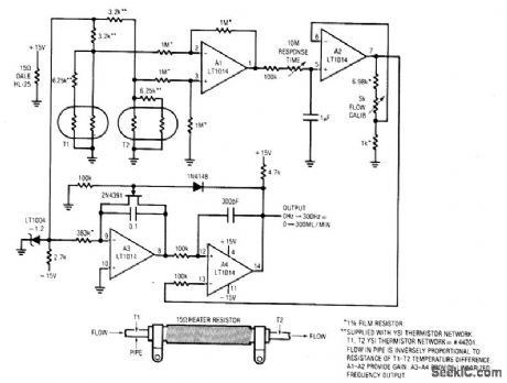
LIQUID_FLOWMETER_1
Published:2009/7/1 1:21:00 Author:May

View full Circuit Diagram | Comments | Reading(467)
RUGGED_LAMP_DRIVER_IS_SHORT_CIRCUIT_PROOF
Published:2009/7/1 1:19:00 Author:May
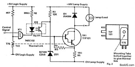
This circuit is capable of driving filament lamps of nominal rating 200 mA at 60 V dc from a CMOS logic signal.The lamp or load is connected in series with the Darlington transistor TR1 and emitter resistor R5. The Zener diode ZD1 establishes a soft reference voltage on the collector of the optical coupler IC2. When the logic control signal from the processor switches the optocoupler on via IC1, base drive is applied to TR1 and the lamp is switched on. (View)
View full Circuit Diagram | Comments | Reading(1729)
LIQUID_FLOWMETER
Published:2009/7/1 1:18:00 Author:May
View full Circuit Diagram | Comments | Reading(541)
PLANT_WATER_GAUGE
Published:2009/7/1 1:17:00 Author:May
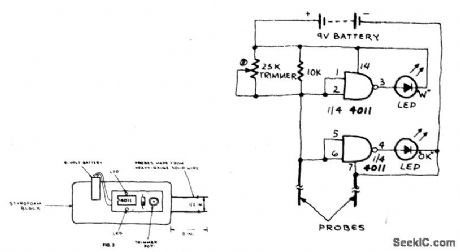
To calibrate the gauge, connect the battery and press the probes gently into a pot containing a plant that is just on the verge of needing water (stick it in so that only an inch of the probe is left visible at the top). Turn the potentiometer until the OK LED lights and then turn it back to the point where that LED goes out and the W , or Water , LED just comes on. The device should now be property adjusted. (View)
View full Circuit Diagram | Comments | Reading(572)
6_DIGIT_STOPWATCH
Published:2009/6/30 22:25:00 Author:May

Low-cost battery-pow-ered electronic stopwatch with 6-digit LED dis-play uses readily available complex-function CM0S ICs to minimize component count. Time range is up to 59 min and 59.99 s. Multiplexing by time-sharing counters through one display-driving decoder cuts battery drain because each digit is on for only one-sixth of time. Article traces operation of circuit step by step. Maxi-mum error is only 0.001 s/h. Four rechargeable nicad batteries Iast 500 h per charge if displays are blanked when not being read, and about 6 h without blanking.-A. Mouton, Build Your Own Digital Stopwatch with Strobed LED Read-out, EDN Magazine, AprilS, 1974, p 55-57. (View)
View full Circuit Diagram | Comments | Reading(3588)
| Pages:305/471 At 20301302303304305306307308309310311312313314315316317318319320Under 20 |
Circuit Categories
power supply circuit
Amplifier Circuit
Basic Circuit
LED and Light Circuit
Sensor Circuit
Signal Processing
Electrical Equipment Circuit
Control Circuit
Remote Control Circuit
A/D-D/A Converter Circuit
Audio Circuit
Measuring and Test Circuit
Communication Circuit
Computer-Related Circuit
555 Circuit
Automotive Circuit
Repairing Circuit