
Index 303
FUZZ_BOX_1
Published:2009/7/1 4:11:00 Author:May

Circuit NotesThe input signal is amplified by the transistors. The distorted output is then clipped by the two diodes and the high frequency noise is filtered from the circuit via the 500 pF capacitor. The 1 M pot adjusts the intensity of fuzz frog maximum to no fuzz (normal the playing). (View)
View full Circuit Diagram | Comments | Reading(783)
1_μS_PULSE
Published:2009/7/1 4:03:00 Author:May

Monostable MVBR converts negative-going event signal into pulses having standardized width of about 1 μs, inverted by 03 for use as input to counter.-T. E. Hutchin-son. Inexpensive Decimal Counting Unit, 73 Magazine. Jan. 1974. p 47-51. (View)
View full Circuit Diagram | Comments | Reading(495)
AMMETER_WITH_SlX_DECADE_RANGE
Published:2009/7/1 4:03:00 Author:May

The Ammeter measures currents from 100 pA to 100 μA without the use of expensive high value resistors. Accuracy at 100 μA is limited by the offset voltage between Q1 and Q2 and, at 100 pA, by the inverting bias current of the LT1008 (View)
View full Circuit Diagram | Comments | Reading(949)
FUZZ_BOX_5
Published:2009/7/1 4:03:00 Author:May

Circuit Notes
Transistors Q1 and Q2 amplify the in- coming signal, and the gain is such that the input will overload when used with an electric guitar. RV1 adjusts the amount of feedback present, and hence voltage gain. The output is, therefore, a squared version of the input signal.The amount of squaring is varied by RV1. (View)
View full Circuit Diagram | Comments | Reading(638)
CALENDAR_CLOCK
Published:2009/7/1 4:01:00 Author:May

Uses Fairchild FCM7001 IC eauivalent of Cal-Tex CT7001 doek chip (which is no Ionger available) to drive six 7-segment LEDs that can be switched to show 12- or 24-h time and 28/30/31 calendar, along with alarm features. Article gives constluction details.Each SN75491 driver chip has pins 3, 5, 10, and 12 connected to pin 11 through 150-ohm resistor RL is typically 2,7K,chosen to limit LED current to less than 5 mA,-W,J. prudhomme,CT7001 Clockbuster,73 magazine,Dec,1976,p 52-54 and 56-58. (View)
View full Circuit Diagram | Comments | Reading(4168)
12_OR_24_h_CLOCK
Published:2009/7/1 3:59:00 Author:May

Single American Microsystems AMI S1736 clock chip drives Iiquidcrystal readout to give either 12-h display with AMjPM indicator or 24-h digital display by changing only three connections.-LSI in Con-sumer Applications, Round 2: Clocks on a Chip, EDN Magazine, May5, 1973, p22-23. (View)
View full Circuit Diagram | Comments | Reading(657)
FUZZ_BOX_4
Published:2009/7/1 3:49:00 Author:May

Circuit Notes
None of the components are particularly critical in value or puality ,as distortion is the sole object! The transistor could be BC107-8-9, 2N2926, etc. (View)
View full Circuit Diagram | Comments | Reading(2587)
FUZZ_BOX_3
Published:2009/7/1 3:47:00 Author:May

Circuit Notes
Q1 and Q2 form a voltage amplifier which has sufficient gain to be overdriven by a rela-tively low input, such as an electric guitar. The result is that the output from Q2 is a Squared-Off verson of the input, giving the required fuzz sound. RV1 adjusts the amount of negative feedback inserted into the circuit by C2, and thus the amount of squaring of the signal. The purpose of R3 and R4 is to lower the output voltage to a suitable level, which is then ad-justed as required with the volume control VR2. (View)
View full Circuit Diagram | Comments | Reading(778)
O_9_s_DIGITAL_READOUT
Published:2009/7/1 3:27:00 Author:May

Can be used for classroom demonstration of digital logic driving 7-segment LED or as attention-getting desk display time base Q1 feeds sequential timing pulses to 7490 decade counter. Pulses are counted in binary mode, and bit pattern corre-sponding to digits 0-9 is fed to 7447 binary-to-decimal decoder/driver connected to 7-segment readout. Calibrate with watch or with timing reference signals from WWV, adjusting R1 so display advances 1 digit per second.-F. M.Mints, Electronic Circuitbook 5: LED Projects, Howard W. Sams, Indianapolis, IN, 1976, p 72-75. (View)
View full Circuit Diagram | Comments | Reading(4983)
4_DIGIT_O7_INCH_LED_DlSPLAY
Published:2009/7/1 2:51:00 Author:May

National MA1013 clock module contains MOS LSI clock IC, display, power supply, and associated discrete components on single printed-circuit board that is easily connected to radio. Operates from either 50-Hz or 60-Hz inputs, and gives either 12- or 24-h display format. Nonmulti-plexed LED drive eliminates RF interference.Display is flashed at 1-Hz rate after powerfailure of any duration, to indicate need for resetting dock. Zero appearing in first digit is blanked. On 12-h version, dot in upper left corner is ener-gized to indicate PM.- MOSiLSl Databook, National Semiconductor, Santa Clara, CA, 1977, p 13-23-13-28.
(View)
View full Circuit Diagram | Comments | Reading(586)
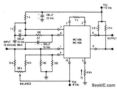
ZENER_REGULATED_FREQUENCY_TO_VOLTAGE_CONVERTER
Published:2009/7/1 2:44:00 Author:May

View full Circuit Diagram | Comments | Reading(456)
555_ASTABLE_WITH_LOW_DUTY_CYCLE
Published:2009/7/1 2:43:00 Author:May

This free-running multivibrator uses an external current sink to discharge the timing capacitor, C. Therefore, interval t2 may easily be 1000 x the pulse duration, t1, which defines a positive output. Capacitor voltage, VC, is a negative going ramp with exponential rise during the pulse output periods. (View)
View full Circuit Diagram | Comments | Reading(623)
PRECISION_REFERENCE_STANDARD_CELL_REPLACEMENT
Published:2009/7/1 2:40:00 Author:May

View full Circuit Diagram | Comments | Reading(482)
PRECISION_REFERENCE_O_V_TO_20_V_POWER_REFERENCE
Published:2009/7/1 2:39:00 Author:May

View full Circuit Diagram | Comments | Reading(558)
RAMP_GENERATOR_WITH_VARIABLE_RESET_LEVEL
Published:2009/7/1 2:39:00 Author:May

View full Circuit Diagram | Comments | Reading(1049)
OSCILLATOR_WITH_DOUBLE_FREQUENCY_OUTPUT
Published:2009/7/1 2:36:00 Author:May
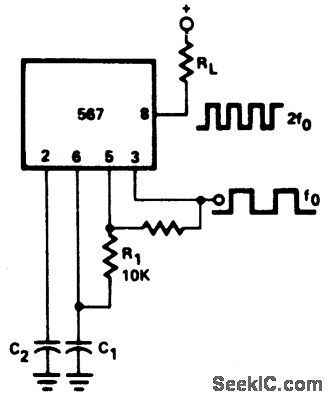
View full Circuit Diagram | Comments | Reading(601)
LOW_FREQUENCY_DOUBLER
Published:2009/7/1 2:34:00 Author:May
View full Circuit Diagram | Comments | Reading(1376)
Ac_driven_bridge_synchronous_demodulator
Published:2009/7/24 5:29:00 Author:Jessie


Figure 4-20 shows a circuit that combines a bridge with a synchronous detector to obtain very high noise rejection capability. Figure 4-21 shows the waveforms. Traces A, B, C, D, E, and F show T1 input, A1 input, LTC1043 clock, A1 output, A2 positive input, and A2 output, respectively. An ac carrier excites the bridge and synchronizes the gain-stage demodulator. In this application, the signal source is a thermistor bridge that detects extremely small temperature shifts in a biochemical microcalorimetry-reaction chamber. To calibrate, adjust the phase pot so that C1 switches when the carrier crosses through zero. LINEAR TECHNOLOGY, APPLICATION NOTE 43, P. 24. (View)
View full Circuit Diagram | Comments | Reading(1792)
Linear_output_thermistor_bridge
Published:2009/7/24 5:17:00 Author:Jessie


Figure 4-11 uses a thermistor in one leg of the bridge circuit. A trim in the opposing leg sets the bridge output to zero at 0℃. A1 and A2 provide additional trimmed gain to furnish a calibrated output. Calibration is performed in similar fashion to the platinum RTD circuits (Figs. 4-9 and 4-10). LINEAR TECHNOLOGY, APPLICATION NOTE 43, P. 17. (View)
View full Circuit Diagram | Comments | Reading(1183)
150_TO_300_MHz_DOUBLER
Published:2009/7/1 2:33:00 Author:May

View full Circuit Diagram | Comments | Reading(458)
| Pages:303/471 At 20301302303304305306307308309310311312313314315316317318319320Under 20 |
Circuit Categories
power supply circuit
Amplifier Circuit
Basic Circuit
LED and Light Circuit
Sensor Circuit
Signal Processing
Electrical Equipment Circuit
Control Circuit
Remote Control Circuit
A/D-D/A Converter Circuit
Audio Circuit
Measuring and Test Circuit
Communication Circuit
Computer-Related Circuit
555 Circuit
Automotive Circuit
Repairing Circuit